Silicide gate transistors and method of manufacture

a semiconductor gate transistor and gate tunneling technology, applied in the field of semiconductor devices, can solve the problems of reduced gate length, high gate resistance, high gate tunneling leakage current, etc., and achieve the effect of improving the performance of the semiconductor devi

Inactive Publication Date: 2006-06-27
TAIWAN SEMICON MFG CO LTD
View PDF10 Cites 53 Cited by
  • Summary
  • Abstract
  • Description
  • Claims
  • Application Information

AI Technical Summary

Benefits of technology

[0015]An objective of the present invention is to provide a transistor structure with an SOI substrate, raised source / drain regions, and a fully silicided gate for improved performance in a semiconductor device.
[0016]A further objective of the present invention is to provide a method for fabricating an SOI transistor with a fully silicided gate that is recessed in one embodiment and not recessed in a second embodiment in order to eliminate boron penetration and gate depletion that is associated with conventional polysilicon gates.
[0018]Yet another objective of the present invention is to decouple the silicidation of the gate and the source / drain regions in a method that achieves full silicidation of a non-recessed gate electrode without degrading the resistance or junction leakage characteristics of the source and drain regions.

Problems solved by technology

Unfortunately, a reduced gate length aggravates the problems of gate depletion, high gate resistance, high gate tunneling leakage current, and boron penetration from a p+ doped gate into the channel region that are associated with polysilicon gates.
This requirement presents a tremendous challenge since the active polysilicon dopant density at the interface of the gate and gate dielectric layer is saturated at 6×10¹⁹ ions / cm3 and 1×10²⁰ ions / cm3, respectively.
Insufficient active dopant density in the gate causes a significant voltage drop across the gate depletion layer and increases the EOT.
As a result, gate capacitance in the inversion regime and inversion charge density (drive current) is reduced or a lower effective gate voltage occurs, thus compromising device performance.
Additionally, a thick silicide region 9b is formed in source / drain regions 4, 5 which is undesirable since it leads to a transistor that suffers from a high source or drain leakage current.
A recent improvement in the design of transistor devices involves raised source and drain regions which increases the thickness of the source and drain regions available for the silicidation process and lowers sheet resistance of the source and drain regions.
However, silicidation occurs only in the raised source / drain regions.
Although the prior art includes several examples of transistors that have at least two of the technology elements that include SOI substrates, raised source / drains, and fully silicided recessed gates, to our knowledge there is no method that incorporates all three elements into a single fabrication scheme.

Method used


Image

  • Silicide gate transistors and method of manufacture
  • Silicide gate transistors and method of manufacture
  • Silicide gate transistors and method of manufacture

Examples


first embodiment

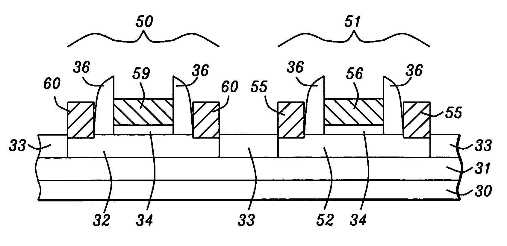
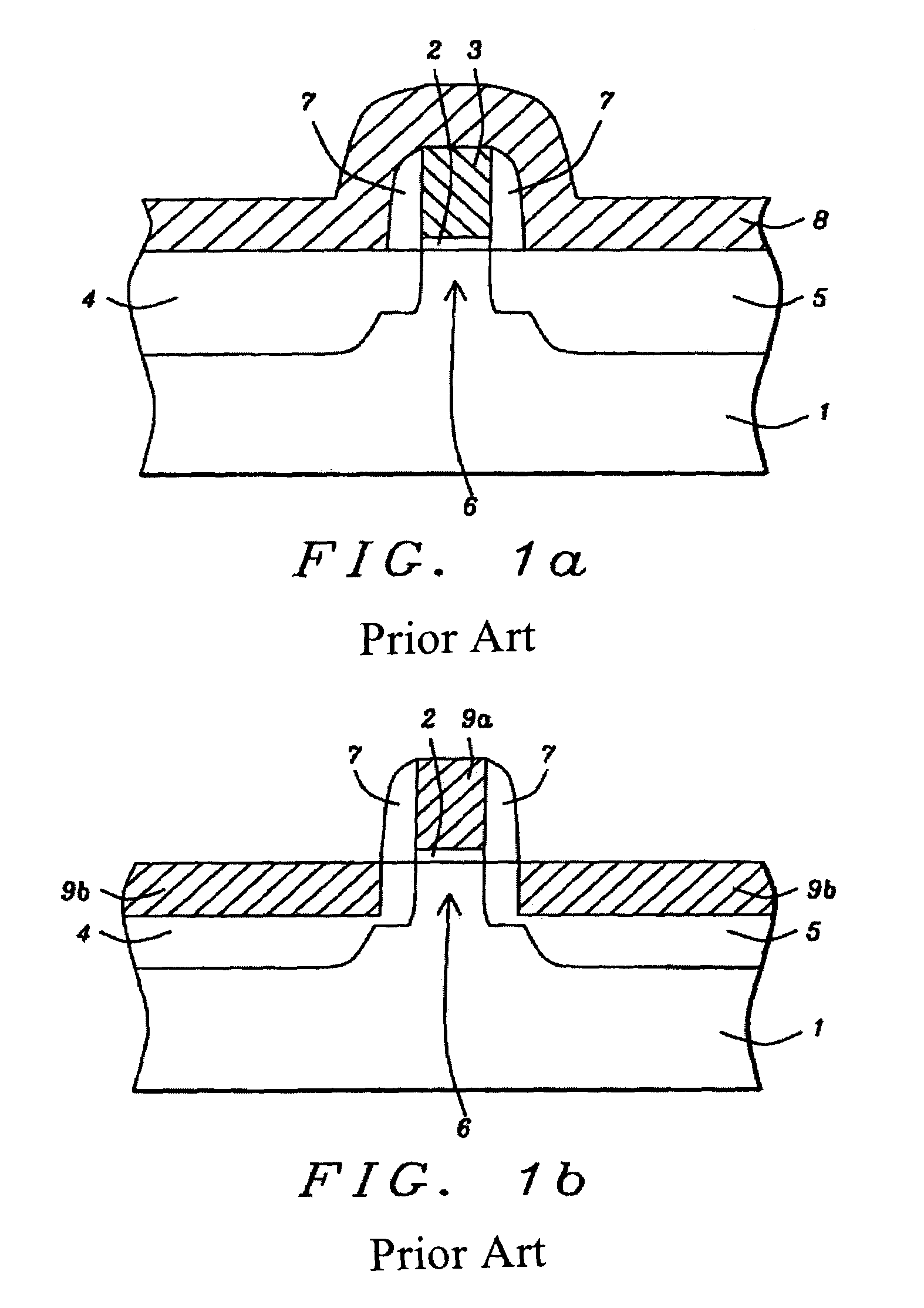
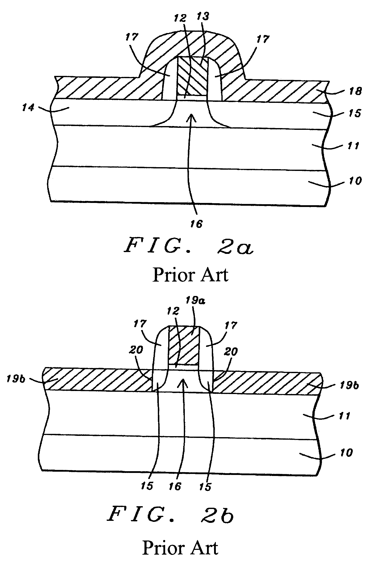
[0031]The present invention generally relates to semiconductor devices with gate electrodes, also referred to as gates, that are fully silicided. More particularly, the invention relates to a transistor having the technology elements of an SOI substrate, a fully silicided gate, and silicided, raised source / drain regions. However, the invention is also useful in forming a transistor that is derived from a bulk semiconductor substrate. In the preferred first embodiment set forth in FIGS. 3a–3e, the silicidation of the gate electrode is decoupled from the silicidation of the raised source / drain regions.

[0032]Referring to FIG. 3a, there is shown a silicon-on-insulator (SOI) substrate that includes a substructure 30, a buried insulator layer 31, and a first semiconductor layer 32. Substructure 30 may contain other active and passive devices that are not shown in order to simplify the drawing. A substrate may be referred to as a chip when the substrate is comprised of more than one device...

second embodiment

[0049]the present invention is a method of fabricating a transistor with a fully silicided, recessed gate electrode in combination with raised source / drain regions that are fully silicided. The method begins with the previously described partially formed transistor shown in FIG. 3a and is continued in FIGS. 4a–4d.

[0050]Referring to FIG. 4a, a second semiconductor layer 44 is preferably selectively deposited by a CVD process on the partially formed transistor structure depicted in FIG. 3a to a thickness that is higher than the spacers 36 and gate electrode 35. The second semiconductor layer 44 is preferably polysilicon but may be amorphous silicon, an alloy such as SiGe, or a compound such as SiGeC. Furthermore, the second semiconductor layer 44 may have a non-planar surface in which the layer is thicker over gate electrode 35 than over the isolation regions 33. A CMP step known to those skilled in the art may be performed to planarize the second semiconductor layer 44 so that the l...


PUM


Abstract

A method in which a gate and raised source / drain (S / D) regions are fully silicided in separate steps to avoid degrading the resistance or junction leakage is described. A gate dielectric layer, gate, and spacers are formed over a semiconductor layer that is preferably Si, SiGe, or SiGeC on a buried insulator. Raised S / D regions are formed by selective epitaxy between spacers and isolation regions. The gate is protected with a mask while the raised S / D regions are covered with a first metal layer. A first anneal affords fully silicided S / D regions. A dielectric stack is deposited on the substrate and planarized to be coplanar with the top of the spacers. The mask is removed and a second metal layer is deposited. A second anneal yields a fully silicided gate electrode. The invention is also an SOI transistor with silicided raised S / D regions and a fully silicided and optionally recessed gate.

Description

FIELD OF THE INVENTION[0001]The present invention relates to a transistor device that combines the elements of fully silicided metal gates, raised source / drain regions, and a silicon-on-insulator substrate. A method of fabricating the transistor device involves decoupling the silicidation of the source and drain region from the gate silicidation for improved performance.BACKGROUND OF THE INVENTION[0002]The demand for greater circuit density and higher performance in Complementary Metal Oxide Semiconductor (CMOS) transistors is driving the gate length (LG) to a smaller dimension that is sub-100 nm in size in advanced technologies. Unfortunately, a reduced gate length aggravates the problems of gate depletion, high gate resistance, high gate tunneling leakage current, and boron penetration from a p+ doped gate into the channel region that are associated with polysilicon gates. To reduce the high gate resistance and gate depletion problems, the active dopant density in the polysilicon ...

Claims


Application Information

Patent Timeline
Patent Type & Authority Patents(United States)
IPC IPC(8): H01L21/336H01L21/3205H01L21/4763H01L21/8238H01L21/84H01L27/12H01L29/45H01L29/49H01L31/0392
CPCH01L21/84H01L27/1203H01L29/66772H01L29/458H01L29/4908H01L29/41783H01L21/823835
Inventor WEN, CHENG-KUOYEO, YEE-CHIATSAO, HSUN-CHIH
Owner TAIWAN SEMICON MFG CO LTD
Why Eureka
Try Eureka