Technique to grow high quality ZnSe epitaxy layer on Si substrate

a technology of znse epitaxy and substrate, which is applied in the direction of polycrystalline material growth, crystal growth process, vacuum evaporation coating, etc., can solve the problems of low single crystal quality of epitaxital films and rough surface of films, and achieves poor mechanical properties, high cost of single crystal ge substrates, and difficult processing.

Inactive Publication Date: 2006-07-04
WITTY MATE CORP
View PDF2 Cites 9 Cited by
  • Summary
  • Abstract
  • Description
  • Claims
  • Application Information

AI Technical Summary

Benefits of technology

[0008]The present process allows to epitaxitally grow high-quality and large-area heterogeneous epitaxital ZnSe materials on Si substrates, which are widely applicable to devices structures as light-emitting diodes, lasers, solar cells, etc. With the present process, ZnSe epitaxital layers with high optic-electrical property, low threading dislocation density and smooth surface are obtained. The production process thereof is simple and low-cost without the disadvantage of out-diffusion of atoms during the epitaxy process, and is able to ideally solve the problems encountered in this art.
[0010]In order to complete the achievement of epitaxitally growing high-quality ZnSe epitaxital layers on Si substrates, which are usable as substrates for growing II–VI groups, and are applicable to devices structures like light-emitting diodes (blue, green or white lights), lasers, solar cells, etc., the present invention provides a process to obtain large-area, high-quality ZnSe epitaxital layers, which can be usable as substrates for growing light-emitting diodes, for example, ZnSe light-emitting diodes which emit blue, green or white lights, or adjustable absorptive light detectors. The above applications are based on the selection of Ge / SiGe / Si (IV group) with compatibility to the lattices and slight thermal expansion coefficiency difference as substrate materials or buffer layers (in other words, materials with compatibility to the lattices and slight thermal expansion coefficiency difference, which include but not limit to II–VI groups heterogeneous epitaxital materials as ZnMgSe, ZnTe, ZnSSe, InSe, CdSe, ZnS, GaSe, etc, in addition to ZnSe). The advantages of the present invention on semiconductor element production process are: to solve the problems like brittle Ge substrates due to their poor mechanical properties, difficult processing works, and higher cost of single-crystal Ge substrates, by using Si as substrate materials (also, Ge is used as buffer layer materials), resulting a greatly simplified production process and reduced cost for growing ZnSe crystalline. The present process is new and of market potential. However, due to the difference of lattice constants, about 4.3%, between Si and Ge and difference between thermal expansion coefficiencies for these materials, a large amount of threading dislocation are created inside SiGe epitaxital layers to lower the single-crystal quality of epitaxital films, resulting rough surfaces of the films.

Problems solved by technology

However, due to the difference of lattice constants, about 4.3%, between Si and Ge and difference between thermal expansion coefficiencies for these materials, a large amount of threading dislocation are created inside SiGe epitaxital layers to lower the single-crystal quality of epitaxital films, resulting rough surfaces of the films.

Method used


Image

  • Technique to grow high quality ZnSe epitaxy layer on Si substrate
  • Technique to grow high quality ZnSe epitaxy layer on Si substrate
  • Technique to grow high quality ZnSe epitaxy layer on Si substrate

Examples


Embodiment Construction

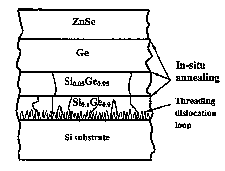
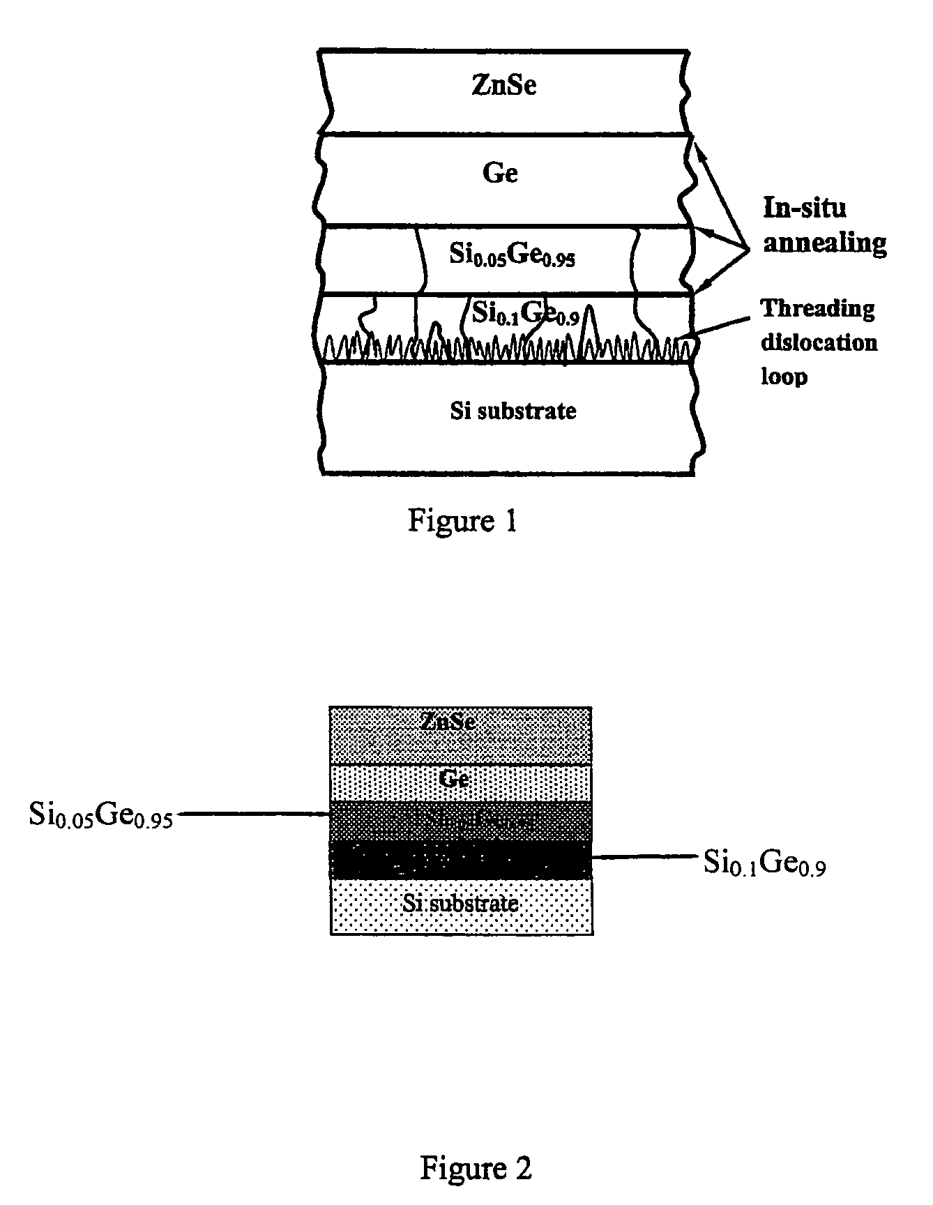
[0018]The present epitaxy is characterized in, first, growing a SiGe epitaxital layer with high Ge mole fraction (for example, 0.5 to 0.8 μm of Si0.1Ge0.9) on an off-cut angle Si substrate, and using this layer to contain a large amount of threading dislocation created by lattice dislocation at the bottom of the layer and interfaces; then growing a second or third SiGe epitaxital layer with higher Ge mole fraction (for example, 0.5 to 0.8 μm of Si0.05Ge0.95, Si0.02Ge0.98), and using the strained interfaces formed between each layer to further terminate the threading dislocation not cleared off on the first layer and propagating upward, eventually growing up a Ge epitaxital layer with a total epitaxital thickness of only few μm, for example, below 3 μm. In the above-described process, a high temperature, i.e., 650 to 800° C., annealing treatment is performed in situ to each layer for 15 to 30 minutes, to further elevate Ge film. Finally, a ZnSe epitaxital layer is grown on the Ge buf...


PUM

PropertyMeasurementUnit
pressureaaaaaaaaaa
thickaaaaaaaaaa
thickaaaaaaaaaa

Abstract

A technique to grow high quality and large area ZnSe layer on Si substrate is provided, comprising growing GexSi1−x / Ge epitaxial layers on Si substrate by using ultra-high vacuum chemical vapor deposition (UHVCVD), and finally growing a ZnSe film on top Ge buffer layers.Two concepts are applied in the process of this invention, the first one is to block the dislocations generated from GexSi1−x epitaxial layers and to terminate the propagated upward dislocations by using strained interfaces, accordingly the dislocation density of ZnSe layer is greatly reduced and the surface roughness is improved; the second concept is to solve the problems of anti-phase domain due to growth of polar materials on non-polar material using off-cut angle Si substrate, and that is free from diffusion problems between different atoms while generally growing ZnSe layers on Si substrate.

Description

FIELD OF THE INVENTION[0001]The present invention relates to a high productive and low-cost technique of heteroepitaxial growth of high-quality and large-area films on Si substrates with lattice mismatch or thermal mismatch; more particularly, to a process of growing II–VI groups materials, for example, ZnSe, on Si substrates. There two techniques are presented in this invention for growth high quality ZnSe on Si. First is to reduce the dislocation density in the ZnSe layers, second is to suppress the impurity inter-diffusion during the growth process by using off-cut Si substrates. The present technique and process are widely applicable to the manufacture of compound semiconductor elements, solar cells and light-emitting diodes, and are usable in integration of IV group and III–V group materials.DESCRIPTION OF THE PRIOR ART[0002]The use of II–VI groups as photoelectric materials, for example, light-emitting diodes, is interested due to their wide band-gap, wherein ZnSe becomes the ...

Claims


Application Information

Patent Timeline
Patent Type & Authority Patents(United States)
IPC IPC(8): H01L21/28H01L21/3205C30B23/08C23C14/06C23C16/30C30B23/02C30B29/48C30B29/52H01L21/00H01L21/06H01L21/10H01L21/203H01L21/205H01L21/365H01L31/0328H01L31/0336H01L31/072H01L31/109
CPCC30B23/02C30B29/48C30B29/52H01L31/0296H01L33/0087H01L21/02631H01L21/0245H01L21/02505H01L21/0256H01L21/02568H01L21/0262H01L21/02381
Inventor YANG, TSUNG-HSILEE, CHUNG-LIANGYANG, CHU-SHOULUO, GUANGLICHOU, WU-CHINGCHANG, CHUN-YENYANG, TSUNG-YEH
Owner WITTY MATE CORP
Why Eureka
Try Eureka