Apparatus and method for high sensitivity read operation

Inactive Publication Date: 2006-07-11
SONY CORP
View PDF4 Cites 26 Cited by
  • Summary
  • Abstract
  • Description
  • Claims
  • Application Information

AI Technical Summary

Benefits of technology

[0024]According to the nonvolatile semiconductor memory device and the method of reading the same according to the present invention, a read operation is performed by using the reverse polarity of the read drain voltage from a write operation, that is, the “reverse read method”, so the read sensitivity is high a corresponding lower voltage read operation is possible. At the same time, since the topmost layer of the gate insulating film is formed by silicon oxynitride, the controllability of the thickne

Problems solved by technology

When the bottom insulating film has a local leakage current path due to a defect, with an FG type memory transistor, most of the stored charges will pass through the leakage path and leak out to the substrate side, so the charge retention characteristic will easily deteriorate.
On the other hand, with a MONOS type memory transistor, since the charge storing means are spatially discrete, only the locally stored charges near the leakage path will pass through the leakage path and locally leak out, so the charge retention characteristic of the entire memory transistor will not easily deteriorate.
An ONO film cannot be formed with good control if incubation time occurs.
If the temperature of form

Method used


Image

  • Apparatus and method for high sensitivity read operation
  • Apparatus and method for high sensitivity read operation
  • Apparatus and method for high sensitivity read operation

Examples


Example

First Embodiment

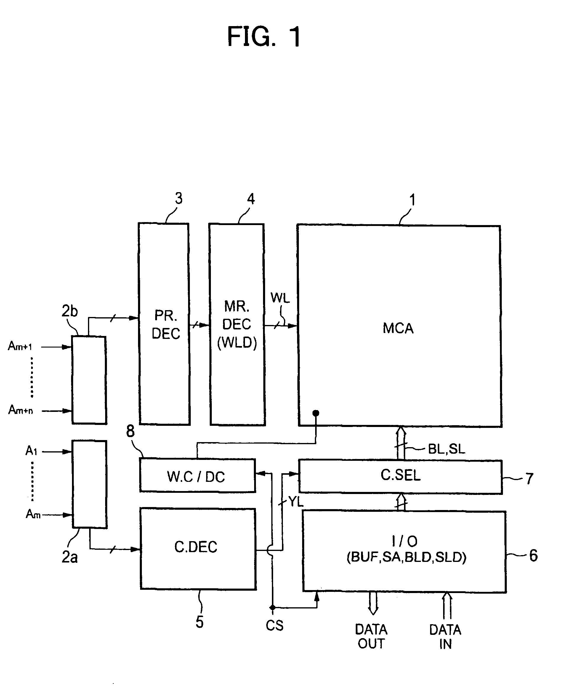
[0038]FIG. 1 shows the schematic configuration of a nonvolatile semiconductor memory device.

[0039]The nonvolatile semiconductor memory device shown in FIG. 1 has a memory cell array (MCA) 1 and memory peripheral circuits controlling operation of the memory cell array 1.

[0040]The memory peripheral circuits include a column buffer 2a, a row buffer 2b, a pre-row decoder (PR.DEC) 3, a main row decoder (MR.DEC) 4, a column decoder (C.DEL) 5, an input / output circuit (I / O) 6, a column gate array (C.SEL) 7, and a well charge / discharge circuit (W.C / DC) 8. Note that, when not performing well bias, the well charge / discharge circuit 8 can be omitted. The memory peripheral circuits, while not particularly illustrated, also include a power source circuit for boosting the power source voltage somewhat if necessary and supplying the main row decoder 4 and the well-charge / discharge circuit 8 with the boosted voltage and a control circuit for controlling the power supply.

[0041]The inp...

Example

Second Embodiment

[0110]In the second embodiment, an alternate metal virtual ground (AMG) type memory cell array shown in FIG. 9 is used. The method of memory cell operation is based on writing data by low voltage hot electrons and erasing data by hot hole injection by the tunnel effect between bands. For example, the method of operation of the first embodiment can be adopted.

[0111]The memory cell array shown in FIG. 9 is comprised of n×m number of memory transistors forming memory cells arranged in a matrix. The gates of the memory transistors arranged in the row directions are connected to the word lines WL1, WL2, or WL3.

[0112]Impurity diffusion layers DR1, DR2, and DR5 are formed in a column direction and are repeated at specific interval in the row direction. The impurity diffusion layers DR1, DR2, and DR5 function as the first or the second source-drain regions and are shared by adjoining memory transistor columns.

[0113]The odd numbered impurity diffusion layers DR1, DR3, and DR...

Example

Third Embodiment

[0123]The third embodiment relates to a nonvolatile semiconductor memory improved in charge injection efficiency and enabling a lower voltage. Here, both a case of storing one bit of data in one memory cell and a case of storing two bits of data in one memory cell will be explained. Note that while the above first embodiment differs in method of writing data from the present embodiment, storage of two bits of data itself is also possible in the first embodiment. Further, the following explanation is based on the cell array of the first embodiment, so FIGS. 1 to 4 are applied to the present embodiment. Note that the cell array of the second embodiment also does not exclude the possibility of application of the method of writing data and the impurity distribution structure of the present embodiment.

[0124]In the present embodiment, two methods are employed for improving the charge injection efficiency.

[0125]The first relates to the write method. Data is written by injec...


PUM


Abstract

A nonvolatile semiconductor memory device enabling a high sensitivity read operation by a low voltage, provided with a gate insulating film comprised of a bottom insulating film, a charge storing film, and a top insulating film successively stacked from the bottom, the bottom insulating film including a silicon oxynitride film directly under the charge storing film, and reading a bit of data stored at a local portion of a sub-source line side of a memory transistor and a bit of data stored at a local portion of a sub-bit line side independently by the reverse read method, whereby the incubation time is suppressed by the presence of silicon oxynitride, the controllability of the thickness of the charge storing film is improved, and the threshold voltage in an erase state is decreased, and a method of high sensitivity reading whereby a lower voltage and improved operational reliability are achieved.

Description

BACKGROUND OF THE INVENTION[0001]1. Field of the Invention[0002]The present invention relates to a nonvolatile semiconductor memory device comprised of a memory transistor between whose channel formation region and gate electrode are provided, in order from the bottom layer, a bottom insulating film, a charge storing film having a charge storing ability, and a top insulating film, and a method of reading the same.[0003]2. Description of the Related Art[0004]Nonvolatile semiconductor memory transistors are roughly divided into floating gate (FG) types with charge storing means for storing charges (floating gates) formed planarly contiguous and for example metal-oxide-nitride-oxide semiconductor (MONOS) types with charge storing means (charge traps etc.) formed planarly discrete.[0005]An FG type nonvolatile semiconductor memory transistor is comprised of a semiconductor substrate or well over which a bottom insulating film, a floating gate (FG) comprised of polycrystalline silicon etc...

Claims


Application Information

Patent Timeline
IPC IPC(8): H01L29/792G11C16/02G11C16/04G11C16/26H01L21/8246H01L21/8247H01L27/10H01L27/115H01L29/788
CPCH01L27/11568H01L27/115H01L27/11521G11C16/26G11C16/0475G11C16/0491H10B43/30H10B69/00H10B41/30
Inventor FUJIWARA, ICHIRONAKAGAWARA, AKIRA
Owner SONY CORP
Why Eureka
Try Eureka