Silicon-on-nothing fabrication process

a technology of silicon and buried oxide, which is applied in the direction of solid-state devices, transistors, coastlines protection, etc., can solve the problems of increasing switching speed, reducing parasitic capacitance of transistors, and exceeding the current manufacturing capabilities of soi wafers, so as to achieve high-performance devices

Inactive Publication Date: 2006-07-18
SHARP KK
View PDF10 Cites 35 Cited by
  • Summary
  • Abstract
  • Description
  • Claims
  • Application Information

AI Technical Summary

Benefits of technology

[0018]In another aspect of the invention, the present invention discloses the fabrication process of a SON device on an isolated floating silicon active area. The SON device is completely isolated from its neighbo

Problems solved by technology

The thin surface silicon layer limits the volume of silicon that needs to be charged to switch the transistor on and off, and therefore reduces the parasitic capacitance of the transistor and increases the switching speed.
However, these requirements on the thickness of the silico

Method used


Image

  • Silicon-on-nothing fabrication process
  • Silicon-on-nothing fabrication process
  • Silicon-on-nothing fabrication process

Examples


Embodiment Construction

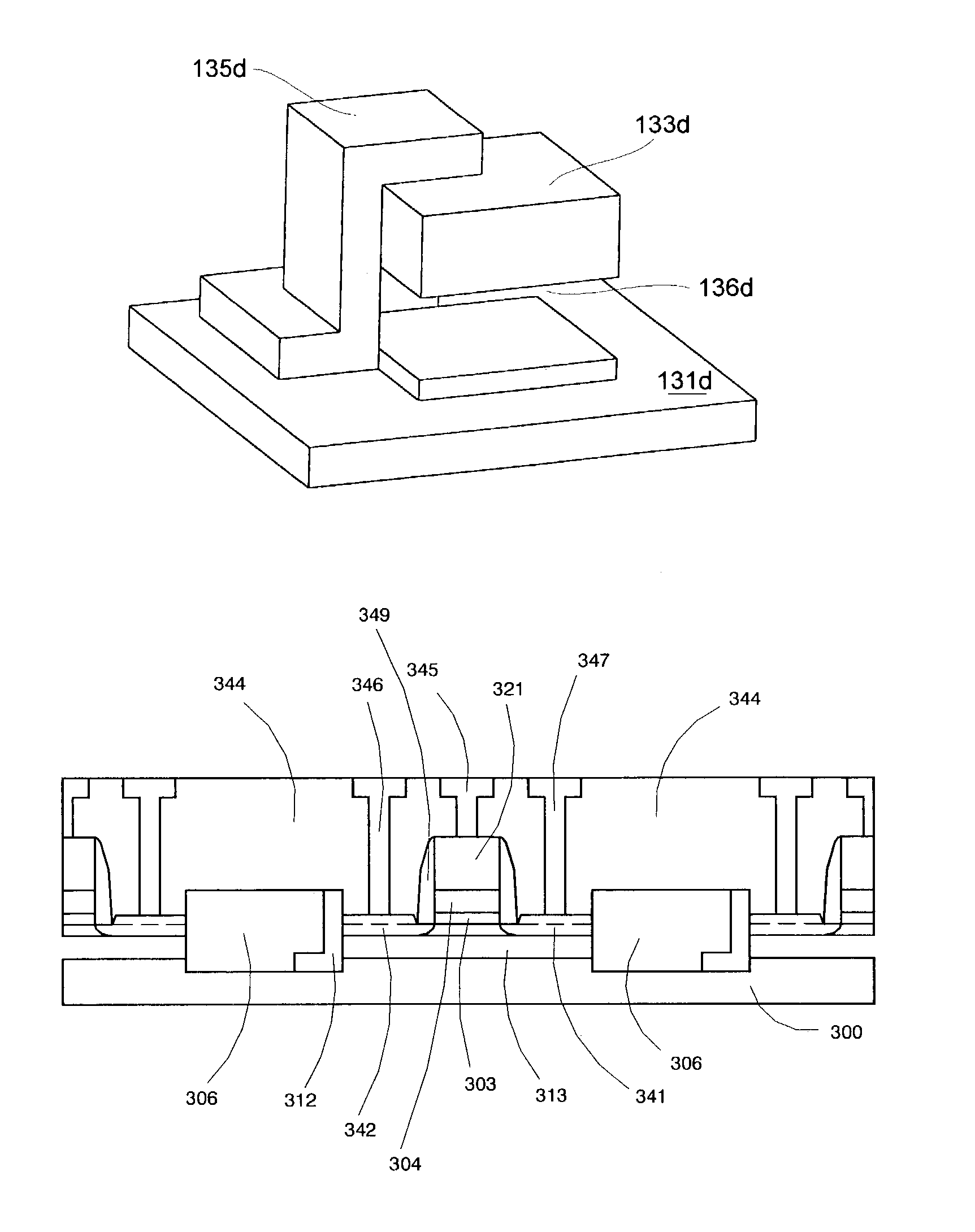
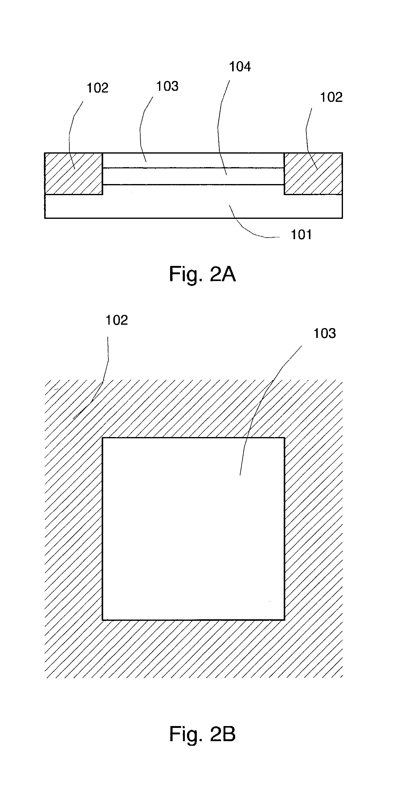
[0029]The present invention discloses a method to fabricate an isolated floating active area on a semiconductor substrate. The isolated floating active area is isolated by trench isolation surrounding the active area and is floated on an air gap. The air gap is made from a sacrificial material and then selectively etched. To prevent the active area from being lift off when the sacrificial layer is removed, a plurality of anchors holding the active area to the substrate is fabricated before the selective etching step. The anchors can then be merged with the isolation material in later step.

[0030]FIG. 2A shows the present invention of an isolated floating active area 103 on a semiconductor substrate 101. The isolated floating active area 103 is isolated by a filled trench isolation 102 surrounding the active area 103 and is isolated from the semiconductor substrate 101 by an air gap 104. The floating active area 103 is supported by the filled trench isolation 102. FIG. 2B shows the to...


PUM


Abstract

A method to fabricate a silicon-on-nothing device on a silicon substrate is provided. The disclosed silicon-on-nothing device is fabricated on an isolated floating silicon active area, thus completely isolated from the silicon substrate by an air gap. The isolated floating silicon active area is fabricated on a silicon germanium layer with a surrounding isolation trench. A plurality of anchors is then fabricated to anchor the silicon active area to the silicon substrate before selectively etching the silicon germanium layer to form the air gap. Isolation trench fill and planarization complete the formation of the isolated floating silicon active area. The silicon-on-nothing device on the isolated floating silicon active area can be polysilicon gate or metal gate and with or without raised source and drain regions.

Description

FIELD OF THE INVENTION[0001]This invention relates to the fabrication of semiconductor devices and silicon-on-insulator (SOI) devices, and specifically to a method for fabricating silicon-on-nothing devices.BACKGROUND OF THE INVENTION[0002]MOSFET fabricated on Silicon-On-Insulator (SOI) substrate has significant advantages such as higher speed, lower power and higher density than on bulk silicon wafer substrate. SOI substrate consists of a thin surface layer of single crystal silicon on an underlayer of insulating material on a bulk silicon wafer. The thin surface silicon layer, typically a few tens of nanometers to several microns thick, is the silicon channel of the transistor. The insulating layer, usually made of silicon dioxide, is referred to as the buried oxide and is usually a few hundreds of nanometers thick.[0003]SOI wafers improve the transistor performance by reducing the operating silicon volume and by isolating the transistors. The thin surface silicon layer limits the...

Claims


Application Information

Patent Timeline
IPC IPC(8): H01L21/336H01L21/762H01L21/76H01L21/764H01L21/84H01L27/12H01L29/786
CPCH01L21/76264H01L21/76283H01L21/76289H01L21/764H01L29/78654H01L27/1203H01L29/66772H01L29/78639H01L21/84E02B8/06E02B8/04E02B7/18
Inventor LEE, JONG-JANHSU, SHENG TENG
Owner SHARP KK
Why Eureka
Try Eureka