Method for design validation of complex IC

a design validation and complex technology, applied in the field of complex design validation, can solve the problems of slow simulation speed, high cost of emulation, and almost impossible chip level design validation, and achieve the effect of reducing cos

Inactive Publication Date: 2006-08-08
ADVANTEST CORP
View PDF5 Cites 23 Cited by
  • Summary
  • Abstract
  • Description
  • Claims
  • Application Information

AI Technical Summary

Benefits of technology

[0032]In the second aspect of the present invention, the method of validating design of complex IC utilized a device model rather than the silicon prototype. The method include the steps of: preparing a device model of an IC to be designed based on IC design data produced under the EDA environment; applying test vectors derived from the IC design data to the device model by an event based test system and evaluating the response output of the device model; modifying test vectors by the event test system to acquire desired response outputs from the device model; and feedbacking the modified test vectors to the EDA environment to modify the IC design data, thereby correcting design errors in the IC design data.
[0033]According to the present invention, design validation is conducted through a method in which the IC simulation model and initial simulation testbench is used together with electronic design automation (EDA) tools to design verification using event based test system. For this purpose, the EDA tools and device simulator are linked to the event based test system to execute the original design simulation vectors and testbench and make modifications in the testbench and test vectors until satisfactory results are obtained. Because EDA tools are linked with the event based test system, these modifications are captured to generate a final testbench that provides satisfactory results. Accordingly, the design validation of the complex IC is achieved without conducting an in-system test of the silicon prototype. Further, the design validation of the complex IC is achieved without using the silicon prototype but using the design model. Therefore, the present invention can achieve significant reduction in the cost and turn around time.

Problems solved by technology

Design validation is one of the most important and difficult tasks in complex IC design because without full functional verification, design errors are not found and removed.
Because of the slow simulation speed and large size of present day designs, chip level design validation is almost an impossible task with the present day tools and methodologies (M. Keating and P. Bricaud, “Reuse methodology manual for system-on-a-chip design”, Kluwer Academic publishers, 0-7923-8175-0, 1998; R. Rajsuman, “System-on-a-Chip: Design and Test”, Artech House Publishers Inc., ISBN 1-58053-107-5, 2000).
Emulation speed is much faster than the speed of co-simulation, although emulation is quite expensive (in general, emulation system cost on the order of 1 million dollars).
Emulation can be close to 1 / 100 of the actual system speed (roughly about 1,000,000 cycles / sec) FPGA (field programmable gate array) or ASIC (application specific integrated circuit) based hardware prototype provides even faster simulation speed, up to 1 / 10 of the actual system speed, but it is even more expensive than emulation as it requires manufacturing of FPGAs or ASICs.
Despite the best attempt by engineers to make the first silicon fully functional, only about 80% designs work correctly when tested at the wafer level, but more than half fail when put into the system for the first time.
The primary reason is the lack of system level testing with sufficient amount of real application run.
Since cycle based test systems (ATE systems) are not able to directly utilize the testbench 58 or VCD file 59 produced under the EDA environment, such verification by IC testers today involves incomplete and inaccurate results.
It is also time consuming to convert the event format data from the EDA environment to the cycle format test pattern data for the cycle based test system.
Since such an in-system test requires both a silicon prototype of the designed chip and a system with application software to run the silicon prototype, it is not only costly but also time consuming.
However, deciding when to use silicon prototype is an important decision as silicon prototype is a costly proposition.
(1) Diminishing bug rate in verification and co-simulation. When the basic bugs are eliminated, extensive application run will be required to find other bugs. Co-simulation and emulation may not be able to run application for extensive time periods.
(2) Difficulty in finding a bug. If finding a bug takes few orders of magnitude more time than the time to fix it, then silicon prototype is very useful, as it will help finding bugs quickly.
(3) Cost (manual effort, time-to-market) of finding bugs. If finding a bug in co-simulation or emulation is extremely costly, then silicon prototyping becomes necessary.
Both FPGA and LPGA lack the gate count capacity and speed of ASICs, thus they are good for smaller blocks, but not suitable for a large complex chip.
In this case, if bug fix demands re-partitioning of the chip, interconnects between FPGAs may require change and hence modifications can be complex.
The design validation method in the conventional technology described above is either extremely high in cost (e.g., method using a silicon prototype) or extremely slow in speed (e.g., method using a co-simulation).
The design validation method today involves different formats between the EDA environment and the tester environment, and thus not able to perform the design validation with high efficiency and accuracy.
Further, the design validation method today requires the in-system test as noted above which involves hardware and software to run the design in an intended system and requires significant feedbacks and interactions between the test environment and the design environment, resulting in a long turnaround time.

Method used


Image

  • Method for design validation of complex IC
  • Method for design validation of complex IC
  • Method for design validation of complex IC

Examples


Embodiment Construction

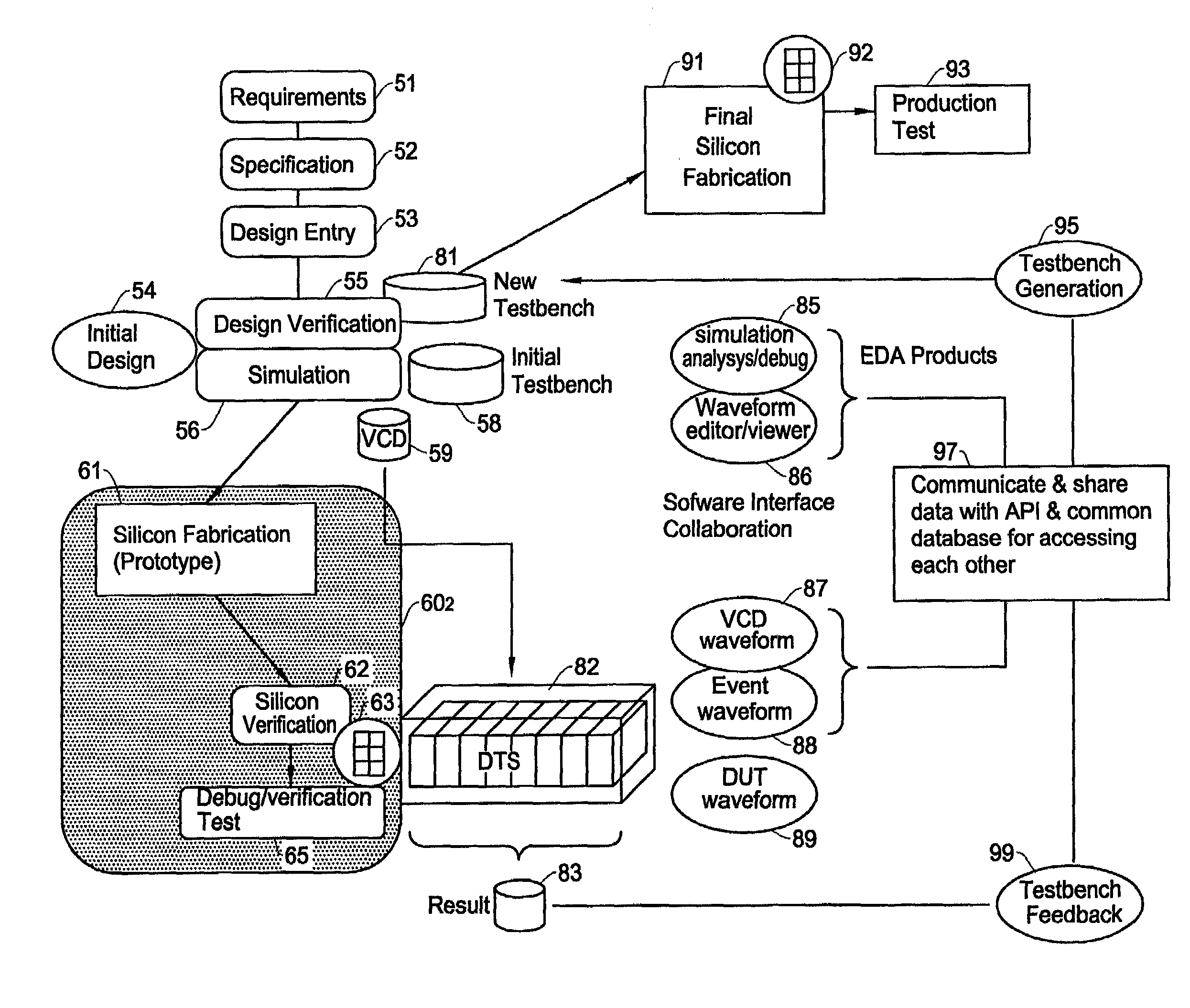
[0041]In the previous applications owned by the same assignee of this invention, an event based test system is described in U.S. patent application Ser. No. 09 / 406,300 (now U.S. Pat. No. 6,532,561) and Ser. No. 09 / 340,371 (now U.S. Pat. No. 6,678,643) “Event based semiconductor test system” and an event based design validation station is described in U.S. patent application Ser. No. 09 / 428,746 (now U.S. Pat. No. 6,678,645) “Method and apparatus for SoC design validation”. Further, a time scaling technology is described in U.S. patent application Ser. No. 09 / 286,226 (now U.S. Pat. No. 6,557,133) “Scaling logic for Event Based Test System”. All of these patent applications are incorporated by reference.

[0042]In the present invention, the inventors provide a concept for IC design verification method using the event based test system. More specifically, in the first embodiment, a method is described for design verification with silicon prototype, and in the second embodiment, a method i...


PUM


Abstract

A method for design validation of complex IC with use of a combination of electronic design automation (EDA) tools and a design test station at high speed and low cost. The EDA tools and device simulator are linked to the event based test system to execute the original design simulation vectors and testbench and make modifications in the testbench and event based test vectors until satisfactory results are obtained. The event based test vectors are test vectors in an event format in which an event is any change in a signal which is described by its timing and the event based test system is a test system for testing an IC by utilizing the event based test vectors. Because EDA tools are linked with the event based test system, these modifications are captured to generate a final testbench that provides satisfactory results.

Description

[0001]This application claims the benefit of Provisional Patent Application No. 60 / 237,001 filed Sep. 29, 2000.FIELD OF THE INVENTION[0002]This invention relates to a method for design validation of complex IC, and more particularly, to a method for evaluating and validating the design of a complex IC such as a system-on-a-chip with use of a combination of electronic design automation (EDA) tools and an event based test system with high speed and low cost.BACKGROUND OF THE INVENTION[0003]At the present time, VLSI design is described in blocks and sub-blocks using a high-level language such as Verilog or VHDL and simulated by behavioral, gate-level Verilog / VHDL simulators. Such simulation is targeted to check the functionality and performance before the design is fabricated into silicon IC.[0004]Design validation is one of the most important and difficult tasks in complex IC design because without full functional verification, design errors are not found and removed. At the same time...

Claims


Application Information

Patent Timeline
Patent Type & Authority Patents(United States)
IPC IPC(8): G06F17/50G01R31/28G01R31/3183G06F11/22G06F11/26
CPCG01R31/318314G06F17/5022G06F11/261G06F30/33
Inventor YAMOTO, HIROAKIRAJSUMAN, ROCHIT
Owner ADVANTEST CORP
Why Eureka
Try Eureka