Diffractive optical device, refractive optical device, illumination optical system, exposure apparatus and exposure method

a technology of refractive optical devices and diffractive optical components, which is applied in the direction of microlithography exposure apparatus, printers, instruments, etc., can solve the problems of unable to contribute to illumination, and reducing the illumination intensity of masks and wafers. , to achieve the effect of reducing the number of light transmissive members, and reducing the number of light transmis

Inactive Publication Date: 2006-08-22
NIKON CORP
View PDF30 Cites 48 Cited by
  • Summary
  • Abstract
  • Description
  • Claims
  • Application Information

AI Technical Summary

Benefits of technology

[0056]Therefore, according to one embodiment, using the illumination field forming device, diffractive optical devices for annular or quadrupole illumination, for example, are positioned in the illumination optical path. In addition, to obtain the annular or quadrupole secondary light source having a desired size (outer diameter) and / or shape (annular ratio) by the optical integrator, the dispersion angle for the angular light beam forming device is configured, and a focal length of the magnification changing optical system is set. As a result, based on the light beam from the light source, the annular or quadrupole secondary light source can be formed without a substantial loss of light amount.
[0057]Furthermore, by changing the dispersion angle by the angular light beam forming device or by changing the focal length of the magnification changing optical system as needed, the size and the annular ratio of the annular or quadrupole secondary light source formed by the optical integrator can be appropriately changed. As a result, various modified illuminations can be performed by appropriately changing the size and the annular ratio of the annular or quadrupole secondary light source without substantial loss of light amount in the formation and restriction of the formation of the annular or quadrupole secondary light sources.
[0058]In particular, the angular light beam forming device is structured from microlens arrays having variable gaps between the arrays, for example, and there is no optical system between the microlens arrays and the illumination field forming device (diffractive optical device). Therefore, using the angular light beam forming device and the illumination field forming device, the number of light transmissive members can be reduced and the illumination optical path can be shortened. As a result, as the entire illumination optical system, because the number of light transmissive members is reduced and the illumination optical path is shortened, the size of the space to be purged is reduced, and loss of light amount due to absorption of light in the illumination optical path is reduced.
[0059]As such, in the illumination optical system of some aspects of the invention, by making the illumination optical system compact based on the simple structure with few members and a short illumination optical path, the loss of light amount due to absorption of light in the illumination optical path can be reduced, and thus various modified illuminations, such as annular illumination and quadrupole illumination, can be performed.
[0060]Moreover, in the exposure apparatus to which the illumination optical system of aspects of the invention is installed, and in the exposure method using the illumination optical system, the mask pattern can be faithfully transferred to the photosensitive substrate under optimum illumination conditions for the mask by using the illumination optical system that can reduce the loss of light amount due to absorption of light in the illumination optical path and perform various modified illuminations, such as annular illumination and quadrupole illumination. Furthermore, excellent micro devices can be manufactured by using the exposure apparatus and the exposure method of this invention, which can faithfully transfer the mask pattern to the photosensitive substrate.

Problems solved by technology

However, when the wavelength of the illumination light is shortened, absorption of that light by light transmissive members can become significant.
Moreover, to achieve the modified illumination (e.g., annular illumination or quadrupole illumination) by limiting the shape of the secondary light source to annular or quadrupole, if the light beam from a relatively large secondary light source formed by a fly's eye lens is merely limited by an aperture diaphragm having an annular or quadrupole aperture, some parts of the light beam from the secondary light source are blocked by the aperture diaphragm, and thus cannot contribute to the illumination (exposure).
As a result, illuminance (exposure intensity) on the mask and the wafer decreases, and the throughput of the exposure apparatus is lowered, due to the loss of light amount caused by the aperture diaphragm.
However, in the illumination optical system having this relatively complex structure, because the number of light transmissive members becomes large, and because the illumination light path becomes long, the space that needs to be purged becomes large and the loss of light amount due to the absorption of light in the illumination light path occurs.

Method used


Image

  • Diffractive optical device, refractive optical device, illumination optical system, exposure apparatus and exposure method
  • Diffractive optical device, refractive optical device, illumination optical system, exposure apparatus and exposure method
  • Diffractive optical device, refractive optical device, illumination optical system, exposure apparatus and exposure method

Examples


first embodiment

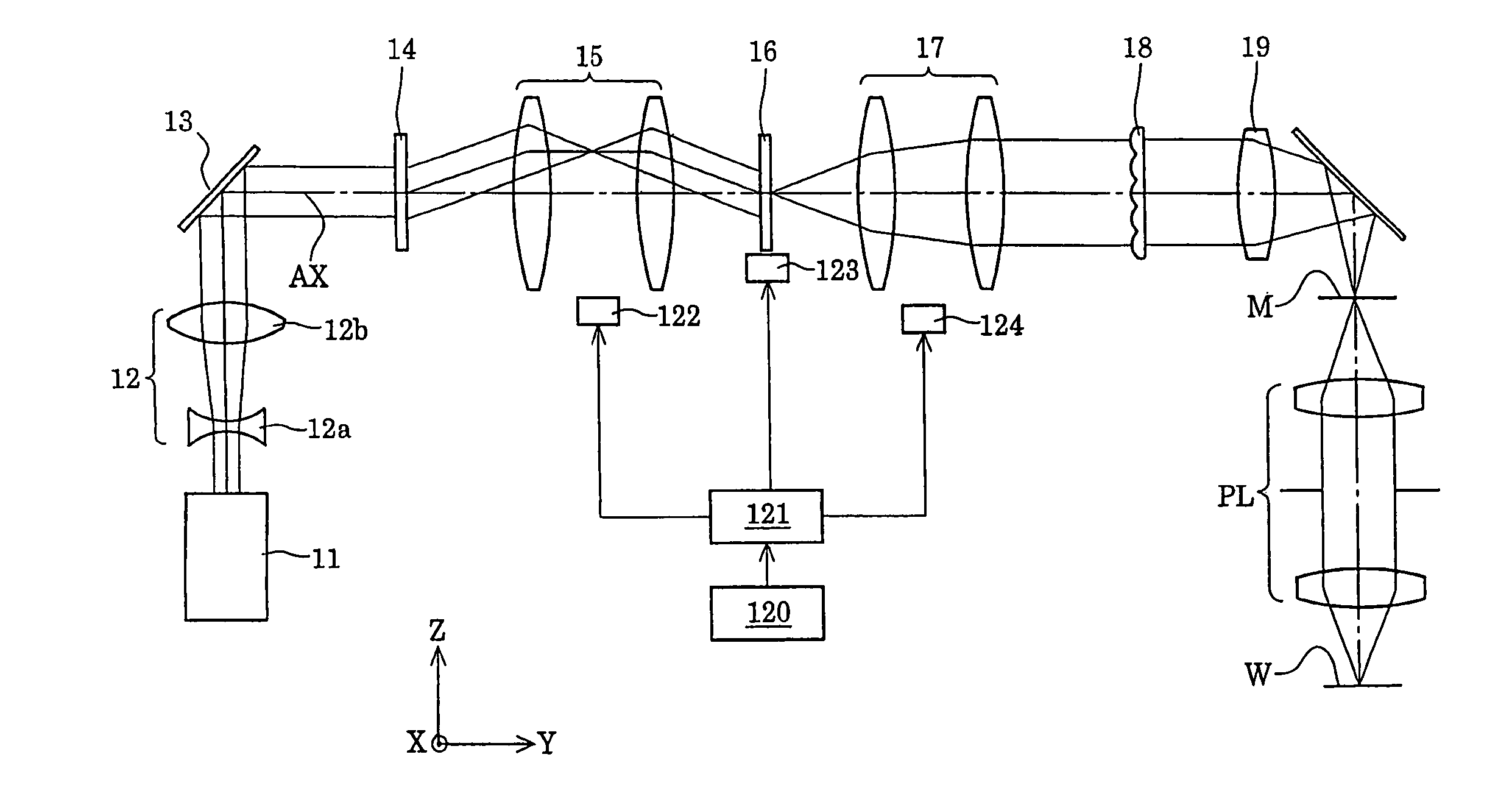
[0099]FIG. 1 is a diagram schematically showing a structure of an exposure apparatus equipped with an illumination optical system according to a first exemplary embodiment of this invention. In FIG. 1, Z, Y and X axes are set respectively in the normal direction (Z axis) of a wafer, which is a photosensitive-material coated substrate, a direction parallel with the plane of the paper of FIG. 1 (Y axis) and within the wafer plane, and a direction perpendicular to the plane of paper of FIG. 1 (X axis) and within the wafer plane.

[0100]The exposure apparatus of FIG. 1 has an ArF excimer laser light source that supplies light having a wavelength of 193 nm, and functions as a light source 11 for supplying exposure light (illumination light). As the light source 11, a KrF excimer laser light source that supplies light having a wavelength of 248 nm, an F2 laser light source that supplies light having a wavelength of 157 nm, a mercury lamp that supplies g-ray (436 nm) or i-ray (365 nm) may al...

second embodiment

[0139]FIG. 7 is a diagram schematically showing a structure of an exposure apparatus equipped with an illumination optical system according to a second exemplary embodiment of this invention. Referring to FIG. 7, the exposure apparatus of the second embodiment includes a light source 21 for supplying exposure light (illumination light). The light source 21 is structured from an ArF excimer laser light source that supplies light having a wavelength of 193 nm, for example, and a beam expander for adjusting the parallel beam emitted from the light source into a light beam having a predetermined rectangular cross-section.

[0140]In addition, a KrF excimer laser light source that supplies light having a wavelength of 248 nm or an F2 laser light source that supplies light having a wavelength of 157 nm may be used as the light source. Moreover, a mercury lamp or a light source that supplies g-rays (436 nm) or i-rays (365 nm) may be used as the light source. When using the mercury lamp, the l...

third embodiment

[0186]FIG. 17 is a diagram schematically showing a structure of an exposure apparatus provided with an illumination optical system according to a third embodiment of this invention. According to the third embodiment, the diffractive optical device of the first embodiment is applied to the diffractive optical device of the illumination field formation portion 23 of the illumination optical system of the second embodiment. The following explains the third embodiment, focusing on its differences from the first embodiment.

[0187]In FIG. 17, on an optical path between a mirror 33 and a diffractive optical device 36, a micro lens array group (or a fly's eye lens group) 340 is arranged, and is constituted by a first microlens array (or a first fly's eye lens: first optical element array) 340a formed by a microlens with positive refractive power, and a second microlens array (or a second fly's eye lens: second optical element array) 340b formed by a microlens with positive refractive power. ...


PUM

PropertyMeasurementUnit
wavelengthaaaaaaaaaa

Abstract

An illumination optical system having a more simplified structure forms various quadrupole-shaped secondary light sources with two-time rotational symmetry with respect to an optical axis. The apparatus can provide illumination conditions that differ in two perpendicular directions on a radiation-receiving plane. In order to form a secondary light source with a quadrupole-shaped light intensity distribution on an illumination pupil plane, a diffractive optical device is provided in which an entrance light beam is converted into four light beams, and a light beam having a shape of four points centered about the optical axis is formed in a far field. The diffractive optical device is provided with a first diffractive optical member that is rotatable about a first axis parallel to the optical axis, and a second diffractive optical member that is rotatable about a second axis parallel to the optical axis, and that is arranged adjacent to the first diffractive optical member. A refractive optical device having first and second refractive optical members accomplishes similar results.

Description

INCORPORATION BY REFERENCE[0001]This is a Continuation-in-Part of International Application No. PCT / JP02 / 12729 filed Dec. 4, 2002, the entire disclosure of which is incorporated herein by reference in its entirety. The disclosures of the following priority applications also are herein incorporated by reference in their entireties: Japanese Patent Application No. 2001-378001 filed Dec. 12, 2001 and Japanese Patent Application No. 2001-378063 filed Dec. 12, 2001.BACKGROUND OF THE INVENTION[0002]1. Field of Invention[0003]This invention relates to diffractive optical devices, refractive optical devices, illumination optical system, exposure apparatus, and exposure methods. In particular, this invention relates to illumination optical system suitable for manufacturing micro-devices, such as semiconductor elements, imaging elements, liquid crystal display elements, and thin film magnetic heads, using lithography processes.[0004]2. Description of Related Art[0005]In typical exposure appar...

Claims


Application Information

Patent Timeline
Patent Type & Authority Patents(United States)
IPC IPC(8): G02B5/18G02B27/10G03B27/54G03F7/20
CPCG03F7/701G03F7/70158G03F7/70108G03F7/70133
Inventor TOYODA, MITSUNORITANITSU, OSAMU
Owner NIKON CORP
Why Eureka
Try Eureka