[0014]According to a third exemplary embodiment of the method of the present invention, a metal layer is irradiated by a first radiation beam pulse having an intensity pattern that includes an array of multiple, relatively small, dot-like shadow regions disposed at respective intersections of regularly spaced, mutually perpendicular diagonal lines, and a beamlet that overlaps all regions of the metal layer not overlapped by the shadow regions. Each region of the metal layer overlapped by the beamlet is melted throughout its entire thickness, while each region of metal layer overlapped by one of the shadow regions remains at least partially unmelted. Each melted region adjoins respective adjacent melted regions. After irradiation by the first radiation beam pulse, each melted region is permitted to cool and resolidify. During resolidification of each melted region, grains grow from each at least partially unmelted region in each adjoining melted region. The spacings of the at least partially unmelted regions, as determined by the spacings of the shadow regions, are such that grains growing from each at least partially unmelted region abut grains growing from neighboring at least partially unmelted regions after the abutting grains have grown by an abutting grain growth distance. After several iterations of irradiation by radiation beam pulses each having the same intensity pattern but shifted with respect to that of a previous pulse, and resolidification of each melted region after each radiation beam pulse, the grain structure of the metal layer comprises generally square single-grain regions with diagonal grain boundaries.
[0015]In accordance with the fourth exemplary embodiment of the method of the present invention, the intensity pattern of each radiation beam pulse includes regularly spaced beamlets in the shape of repeating chevrons where adjacent repeating chevron-shaped beamlets are staggered with respect to one another such that the peaks of each repeating chevron-shaped beamlet are aligned with respective troughs of adjacent repeating chevron-shaped beamlets, and the troughs of each repeating chevron-shaped beamlet are aligned with respective peaks of adjacent repeating chevron-shaped beamlets. The intensity pattern of each radiation beam pulse also includes shadow regions each positioned in between and adjoining respective adjacent beamlets. When a metal layer is irradiated by a radiation beam pulse having such an intensity pattern, each region overlapped by a respective one of the beamlets is melted throughout its entire thickness, and each region overlapped by a respective one of the shadow regions remains at least partially unmelted. Each one of the melted regions has the shape of a repeating chevron with opposing at least partially unmelted edges. After irradiation by the radiation beam pulse, each one of the melted regions cools and resolidifies. During resolidification of each melted region, grains grow from each of the opposing edges of the melted region in opposite directions towards one another in the melted region until the grains growing from the opposing edges abut one another along approximately the center line of the repeating chevron-shaped melted region after the abutting grains have grown by a characteristic growth distance. The beamlets and shadow regions of the intensity pattern of a further radiation beam pulse are shifted with respect to the metal layer in the direction of the peaks of the repeating-chevron-shaped beamlets by a distance less than the characteristic growth distance. The grain structure obtained after multiple iterations of irradiation and resolidification has adjoining single grain regions each having a generally hexagonal shape.
[0016]According to a fifth exemplary embodiment of the method of the present invention, the intensity pattern of the first radiation beam pulse has a plurality of regularly spaced, relatively narrow, linear, stripe-like shadow regions, and a plurality of regularly spaced, relatively wide, linear, stripe-like beamlets, each one of the beamlets being positioned in between and adjoining respective adjacent shadow regions. When a metal layer is irradiated by the first radiation beam pulse, each region of the metal layer overlapped by a respective one of the beamlets is melted throughout its entire thickness, and each region of the metal layer overlapped by a respective one of the shadow regions remains at least partially unmelted. Each at least partially unmelted region adjoins respective adjacent melted regions. After irradiation by the first radiation beam pulse, each melted region of the metal layer is permitted to resolidify. During resolidification of each melted region, respective grains grow therein from adjoining at least partially unmelted regions in opposite directions towards one another, and abut one another along a respective one of a plurality of first grain abutment boundaries after the abutting grains have grown by a first abutting grain growth distance. After completion of resolidification following irradiation by the first radiation beam pulse, the metal layer is irradiated by a second radiation beam pulse having the same intensity pattern as the first radiation beam pulse, but where the shadow regions and beamlets thereof are shifted in a direction perpendicular to the first grain abutment boundaries by a distance at least equal to the width of the shadow regions but less than the first abutting grain growth distance. When the metal layer is irradiated by the second radiation beam pulse, each region of the metal layer overlapped by a respective one of the shifted beamlets is melted throughout its entire thickness, and each region of the metal layer overlapped by a respective one of the shifted shadow regions remains at least partially unmelted. Each at least partially unmelted region adjoins respective adjacent melted regions. After irradiation by the second radiation beam pulse, the melted regions of the metal layer are permitted to cool and resolidify. During resolidification of each melted region, respective single grains grow therein from adjoining at least partially unmelted regions in opposite directions towards one another, and abut one another along a respective one of a plurality of second grain abutment boundaries after the abutting single grains have grown by the first abutting grain growth distance. Upon completion of resolidification of the melted regions after irradiation by the second radiation beam pulse, the metal layer has a grain structure comprising relatively long single grains extending between respective adjacent second grain abutment boundaries and having lateral grain boundaries approximately perpendicular to the second grain abutment boundaries.
[0017]According to a sixth exemplary embodiment of the method of the present invention, after completion of resolidification of the melted regions of the metal layer following irradiation by the second radiation beam pulse in the fifth exemplary embodiment described above, the metal layer on the substrate is rotated by 90° with respect to the second grain abutment boundaries. The rotated metal layer is then irradiated with a third radiation beam pulse having an intensity pattern that includes a plurality of regularly spaced, relatively narrow, linear, stripe-like shadow regions, each one being perpendicular to the second grain abutment boundaries of the grain structure of the rotated metal layer, and a plurality of regularly spaced, relatively wide, linear stripe-like beamlets also perpendicular to the second grain abutment boundaries. Each one of the beamlets is positioned in between and adjoining respective adjacent shadow regions. When each point on the rotated metal layer is irradiated by the third radiation beam pulse, each region of the metal layer overlapped by a respective one of the beamlets is melted throughout its entire thickness, and each region of the metal layer overlapped by a respective one of the shadow regions remains at least partially unmelted. Each at least partially unmelted region adjoins respective adjacent melted regions. After irradiation by the third radiation beam pulse, each melted region of the metal layer is permitted to cool and resolidify. During resolidification of each melted region, different single grains grow from each at least partially unmelted region into each adjoining melted region, and in each melted region respective grains grow from adjoining at least partially unmelted regions in opposite directions towards one another, and abut one another along a respective one of a plurality of second grain abutment boundaries after the abutting single grains have grown by a second abutting grain growth distance. The abutting single grains each have a dimension along the third grain abutment boundaries equal to the distance between adjacent second grain abutment boundaries. After completion of resolidification of the melted regions of the metal layer after irradiation by the third radiation beam pulse, each point on the metal layer is irradiated by a fourth radiation beam pulse having the same intensity pattern as the third radiation beam pulse, but where the shadow regions and beamlets thereof are shifted in a direction perpendicular to the third grain abutment boundaries by a distance at least equal to the width of the shadow regions but less than the second abutting grain growth distance. When each point on the metal layer is irradiated by the fourth radiation beam pulse, each region of the metal layer overlapped by a respective one of the shifted beamlets is melted throughout its entire thickness, and each region of the metal layer overlapped by a respective one of the shifted shadow regions remains at least partially unmelted. Each at least partially unmelted region adjoins respective adjacent melted regions. After irradiation by the fourth radiation beam pulse, each melted region of the metal layer is permitted to cool and resolidify. During resolidification of each melted region, respective single grains grow from each at least partially unmelted region into each adjoining melted region, and in each melted region respective single grains grow from adjoining at least partially unmelted regions in opposite directions towards one another, and abut one another along a respective one of a plurality of fourth grain abutment boundaries after the abutting single grains have grown by the second abutting grain growth distance. Upon completion of resolidification of the melted regions after irradiation by the fourth radiation beam pulse, the metal layer has a grain structure comprising an array of generally rectangular-shaped single-grain regions in respective rows and columns, each rectangular-shaped single-grain region having a dimension on two opposite sides equal to the distance between adjacent second grain abutment boundaries and having a dimension on the other two opposite sides equal to the distance between adjacent fourth grain abutment boundaries.
[0018]According to a seventh exemplary embodiment of the method of the present invention, the metal layer is in the form of a relatively narrow metal layer strip having a predefined contour. The width of the relatively narrow metal layer strip is sufficiently small so as to allow only single grains to grow therein. The metal layer strip is irradiated by a first radiation beam pulse having an intensity pattern that includes a plurality of relatively narrow, linear, stripe-like shadow regions positioned at regular intervals along the metal layer strip and a beamlet overlapping all regions of the metal layer strip not overlapped by a respective one of the shadow regions. Each region of the metal layer strip overlapped by the beamlet is melted throughout its entire thickness, and each region of the metal layer strip overlapped by a respective one of the shadow regions remains at least partially unmelted. Each at least partially unmelted region adjoins respective adjacent melted regions. After irradiation by the first radiation beam pulse, each melted region of the metal layer strip is permitted to cool and resolidify. During resolidification of each melted region, different single grains grow from each at least partially unmelted region in each adjoining melted region, and in each melted region respective single grains grow from adjoining at least partially unmelted regions in opposite directions towards one another, and abut one another at a respective one of a plurality of first grain abutment boundaries after the abutting single grains have grown by an abutting grain growth distance. After completion of resolidification of each melted region following irradiation by the first radiation beam pulse, the metal layer strip is irradiated with a second radiation beam pulse having the same intensity pattern as the first radiation beam pulse, but where each one of the shadow regions is shifted along the metal layer strip by a distance greater than the width of the shadow regions but less than the abutting grain growth distance. The beamlet of the intensity pattern of the second radiation beam pulse is also shifted with respect to the metal layer but still overlaps all regions of the metal layer strip not overlapped by the shadow regions. When the metal layer strip is irradiated by the second radiation beam pulse, each region of the metal layer strip overlapped by the shifted beamlet is melted throughout its entire thickness, and each region of the metal layer strip overlapped by a respective one of the shifted shadow regions remains at least partially unmelted. Each at least partially unmelted region adjoins respective adjacent melted regions. After irradiation by the second radiation beam pulse each melted region of the metal layer strip is permitted to cool and resolidify. During resolidification of each melted region, a respective single grain grows from each at least partially unmelted region in each adjoining melted region, and in each melted region respective single grains grow from adjoining at least partially unmelted regions in opposite directions towards one another, and abut one another at a respective one of a plurality of second grain abutment boundaries after the abutting single grains have grown by the abutting grain growth distance. After completion of resolidification of each melted region following the irradiation by the second radiation beam pulse, the metal layer strip has a grain structure comprising regions of single grains extending between respective adjacent ones of the second grain abutment boundaries. Each second grain abutment boundary is substantially perpendicular to the metal layer strip at the location of each second grain abutment boundary.
[0019]According to an eighth exemplary embodiment of the method of the present invention, the metal layer comprises at least one relatively narrow metal layer strip having at least one segment and a respective predefined contour having a Manhattan geometry. The width of each one of the at least one relatively narrow metal layer strip is sufficiently small so as to permit only single grains to grow therein. Each one of the at least one metal layer strip is irradiated by a first radiation beam pulse having an intensity pattern that includes a plurality of regularly spaced, relatively narrow, linear, stripe-like shadow regions, and a plurality of regularly spaced, relatively wide, linear, stripe-like beamlets. Each one of the beamlets is positioned in between and adjoining respective adjacent shadow regions. Each segment of each one of the at least one metal layer strip is diagonally oriented with respect to the shadow regions and the beamlets. When each one of the at least one metal layer strip is irradiated by the first radiation beam pulse, each region of the metal layer strip overlapped by a respective one of the beamlets is melted throughout its entire thickness, and each region of the at least one metal layer strip overlapped by a respective one of the shadow regions remains at least partially unmelted. Each at least partially unmelted region adjoins respective adjacent melted regions. Following irradiation by the first radiation beam pulse, each melted region of each one of the at least one metal strip is permitted to cool and resolidify. During resolidification of each melted region, different single grains grow from each at least partially unmelted region in each adjoining melted region, and in each melted region respective single grains grow from adjoining at least partially unmelted regions in opposite directions towards one another, and abut one another at a respective one of a plurality of first grain abutment boundaries after the abutting single grains have grown by an abutting grain growth distance. Each one of the first grain abutment boundaries is approximately parallel to the shadow regions and the beamlets. After completion of resolidification of each melted region of each one of the at least one metal layer strip following irradiation by the first radiation beam pulse, each one of the at least one metal layer strip is irradiated by a second radiation beam pulse having the same intensity pattern as the first radiation beam pulse, but where the shadow regions and beamlets thereof are each shifted in a direction perpendicular to the first grain abutment boundaries by a distance at least equal to the width of the shadow regions but less than the distance that would cause the shifted shadow regions to overlap the first grain boundaries. When each one of the at least one metal layer strip is irradiated by the second radiation beam pulse, each region of each one of the at least one metal layer strip overlapped by a respective one of the shifted beamlets is melted throughout its entire thickness, and each region of the at least one metal layer strip overlapped by a respective one of the shifted shadow regions remains at least partially unmelted. Each at least partially unmelted region adjoins respective adjacent melted regions. After irradiation by the second radiation beam pulse, each melted region of each one of the at least one metal layer strip is permitted to cool and resolidify. During resolidification of each melted region, a respective single grain grows from each at least partially unmelted region in each adjoining melted region, and in each melted region, respective single grains grow from adjoining at least partially unmelted regions in opposite directions towards one another, and abut one another at a respective one of a plurality of second grain abutment boundaries after the abutting single grains have grown by the abutting grain growth distance. Each one of the second grain abutment boundaries is approximately parallel to the shifted shadow regions and the shifted beamlets. After completion of resolidification of each melted region following irradiation by the second radiation beam pulse, each one of the at least one metal layer strip has a grain structure comprising regions of single grains extending between respective adjacent second grain abutment boundaries. Each second grain abutment boundary is perpendicularly oriented in relation to a respective one of the at least one metal layer strip at the location of the second grain abutment boundary.


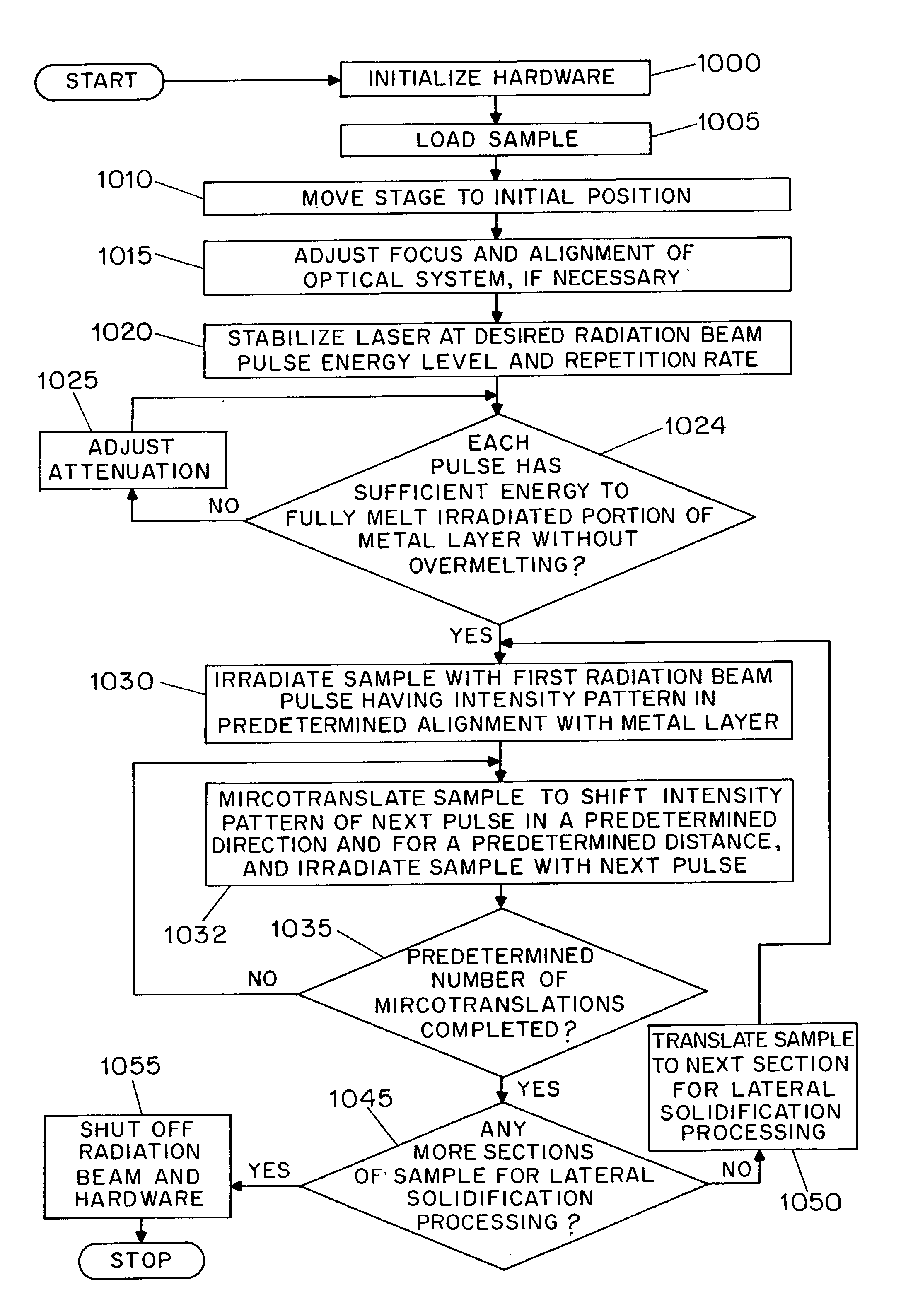
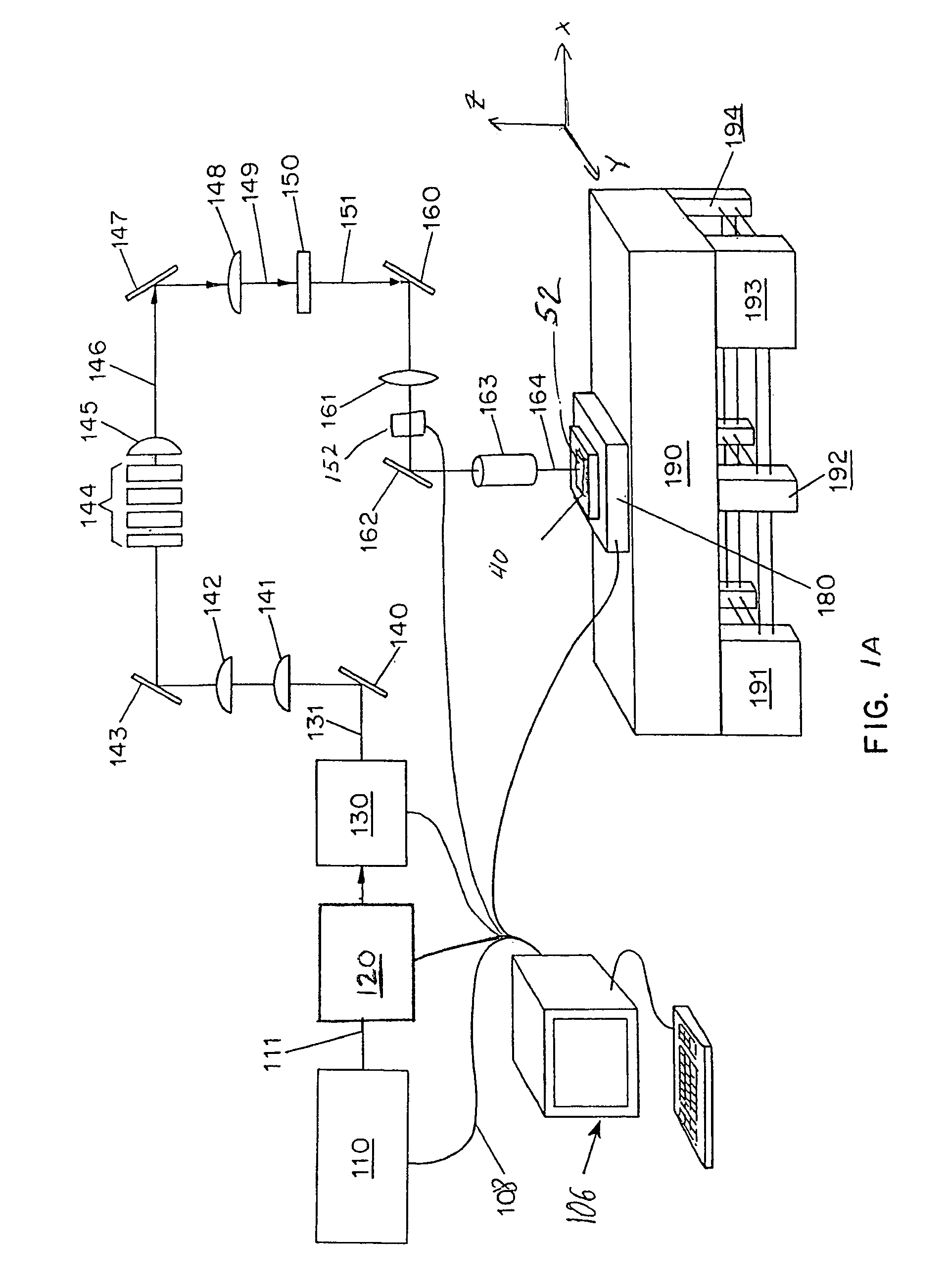
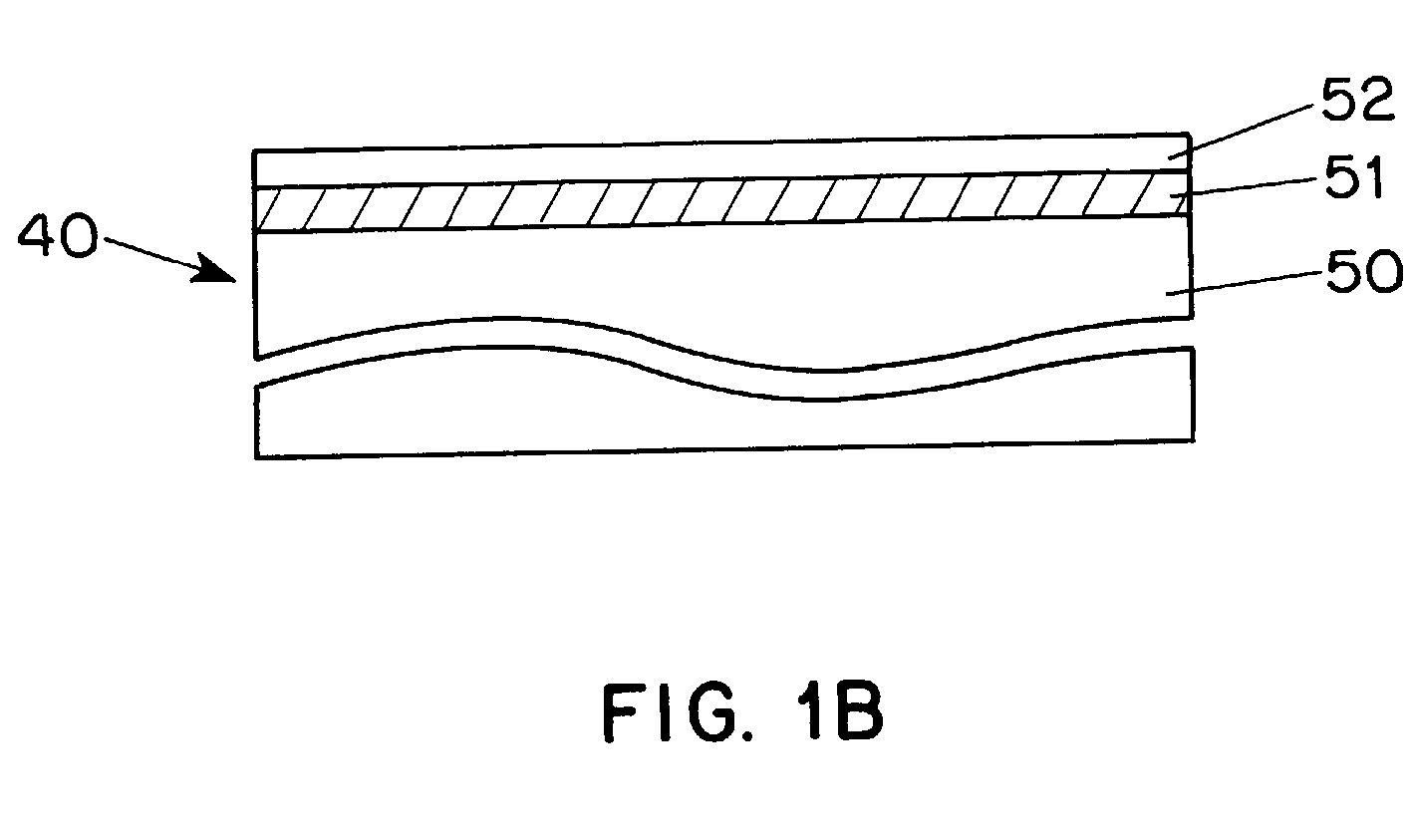