Magnetic tunnel junctions for MRAM devices

a tunnel junction and magnetic tunnel technology, applied in semiconductor devices, solid-state devices, instruments, etc., can solve the problems of reducing resistance, deterioration of various parts and reducing magnetoresistance and/or resistance, so as to reduce or eliminate neel coupling, improve device yield, and improve thermal stability of mtj memory cells

Active Publication Date: 2006-12-12
IBM CORP +1
View PDF8 Cites 47 Cited by
  • Summary
  • Abstract
  • Description
  • Claims
  • Application Information

AI Technical Summary

Benefits of technology

[0012]These and other problems are generally solved or circumvented, and technical advantages are generally achieved, by preferred embodiments of the present invention, which provide methods of manufacturing improved MTJ memory cells and structures thereof. The MTJ cell is comprised of a first and a second magnetic layer disposed on either side of a tunnel barrier layer. In one embodiment, a diffusion barrier formed from one or more thin layers of an amorphous ferromagnetic material are inserted within or at the surfaces of the first and second magnetic layers of an MTJ memory cell, resulting in improved performance of the MTJ cell particularly with regard to an increased thermal stability. In another embodiment, a diffusion barrier is disposed between an anti-ferromagnetic layer and an anti-parallel layer of a first magnetic layer of an MTJ memory cell. The diffusion barrier is comprised of an amorphous ferromagnetic material or may also be comprised of a nickel-iron (NiFe) alloy such as permalloy. A pinned layer of the anti-parallel layer may comprise a NiFe alloy diffusion barrier, in one embodiment. An amorphous material layer may be disposed within the second magnetic layer, or between the tunnel barrier layer and the first magnetic layer, or both, resulting in improved thermal stability and reduced Neel coupling for an MTJ memory cell.
[0017]Advantages of embodiments of the present invention include reducing or eliminating Neel coupling and improving thermal stability of MTJ memory cells, which results in improved device yields and cost savings.

Problems solved by technology

Because MRAM devices operate differently than traditional memory devices, they introduce design and manufacturing challenges.
When heated to temperatures above about 350 degrees C., or lower or higher than 350 degrees C., depending on the composition of the manganese containing layer, manganese can diffuse into other layers of an MTJ memory cell, causing deterioration of various parts of the MTJ memory cell.
For example, it is possible that the magnetic reference system may be weakened or, more likely, the Mn diffuses to or even through the tunnel barrier which can result in diminished magnetoresistance and / or lowered resistance, effectively destroying the functioning of the MTJ memory cell.
Another problem confronted in MRAM manufacturing is Neel coupling between nearby magnetic material layers.
Neel coupling results in a resistive memory element that is magnetically asymmetrical and therefore, favors one state of the memory over the other state, making the memory device difficult to operate.

Method used


Image

  • Magnetic tunnel junctions for MRAM devices
  • Magnetic tunnel junctions for MRAM devices
  • Magnetic tunnel junctions for MRAM devices

Examples


Embodiment Construction

[0029]The making and using of the presently preferred embodiments are discussed in detail below. It should be appreciated, however, that the present invention provides many applicable inventive concepts that can be embodied in a wide variety of specific contexts. The specific embodiments discussed are merely illustrative of specific ways to make and use the invention, and do not limit the scope of the invention.

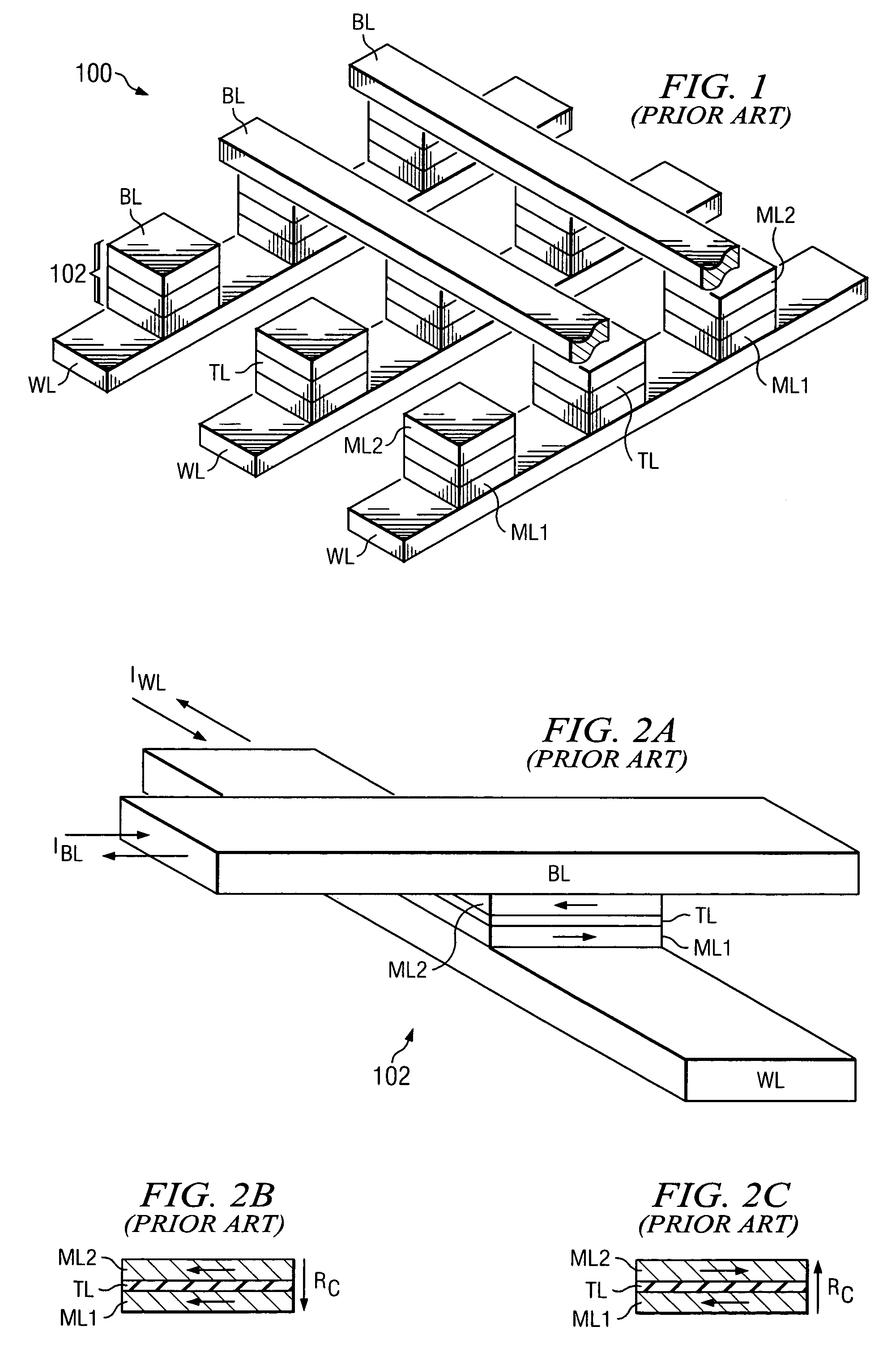
[0030]The present invention will be described with respect to preferred embodiments in a specific context, namely magnetic memory cells of an MRAM device. Embodiments of the present invention may also be applied, however, to other magnetic memory cell designs and magnetic semiconductor device applications, as well as magnetic hard disk drive recording read heads and sensors.

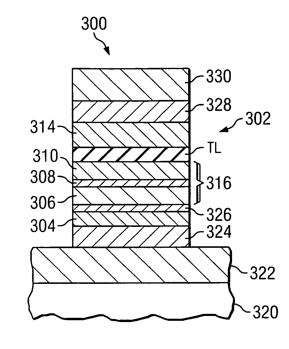
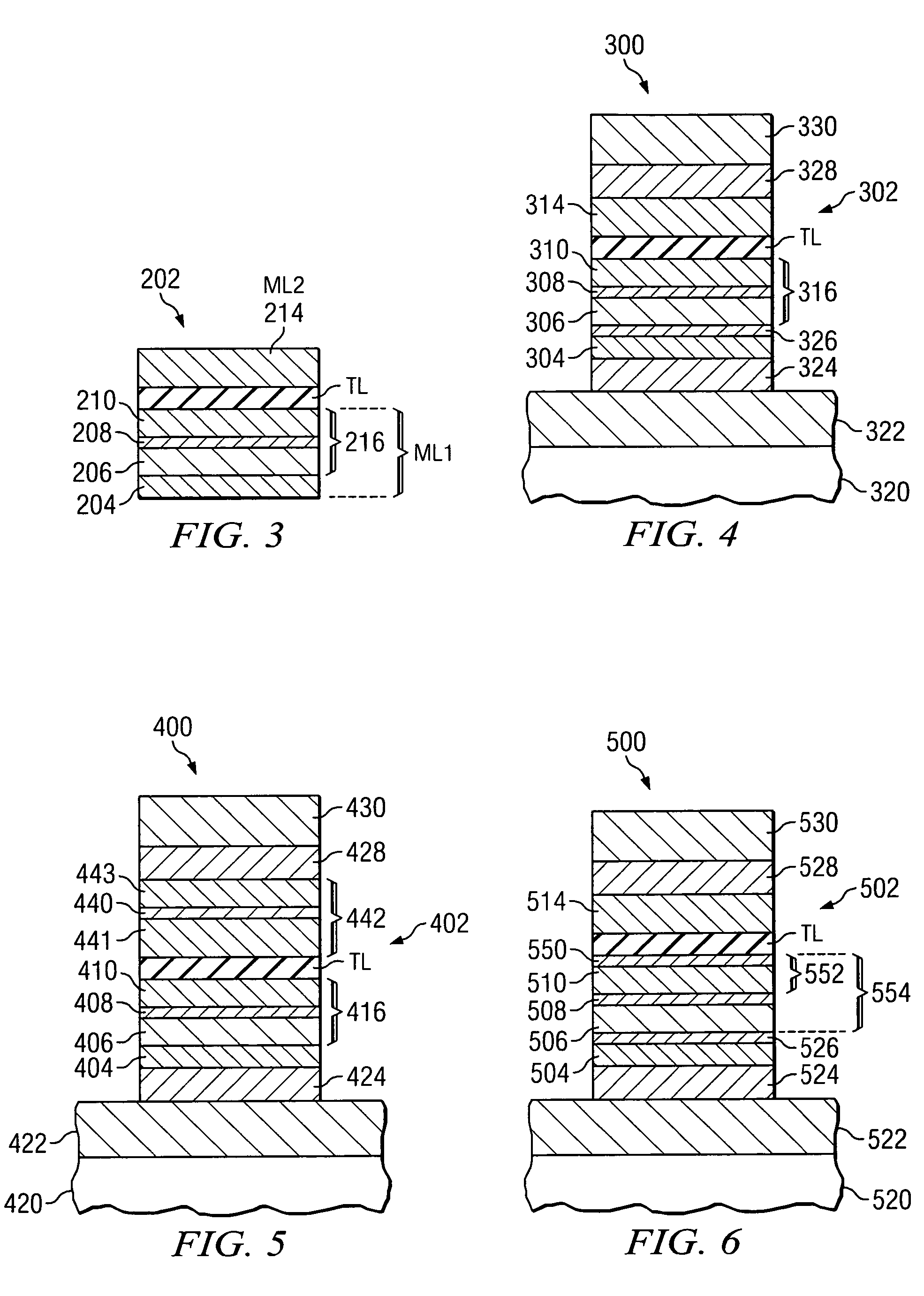
[0031]FIG. 3 shows a cross-sectional view of a less-preferred design of an MTJ memory cell 202. The MTJ memory cell 202 comprises a first magnetic layer ML1, a tunnel barrier layer (TL) disposed over the f...


PUM

PropertyMeasurementUnit
temperaturesaaaaaaaaaa
anti-ferromagneticaaaaaaaaaa

Abstract

Methods of manufacturing MTJ memory cells and structures thereof. A diffusion barrier is disposed between an anti-ferromagnetic layer and a pinned layer of an MTJ memory cell to improve thermal stability of the MTJ memory cell. The diffusion barrier may comprise an amorphous material or a NiFe alloy. An amorphous material may be disposed adjacent a bottom surface of a tunnel junction, within a free layer, or both. An MTJ memory cell with improved thermal stability and decreased Neel coupling is achieved.

Description

TECHNICAL FIELD[0001]The present invention relates generally to semiconductor memory devices, and more particularly to magnetic tunnel junctions (MTJ's) used as storage elements in magnetic random access memory (MRAM) devices and methods of manufacture thereof.BACKGROUND[0002]Semiconductors are used in integrated circuits for electronic applications, including radios, televisions, cell phones, and personal computing devices, as examples. One type of semiconductor device is a semiconductor storage device, such as a dynamic random access memory (DRAM) or a flash memory, both of which use charge to store information.[0003]A more recent development in semiconductor memory devices involves spin electronics, which combines semiconductor technology and magnetic materials and devices. The spins of electrons, through their magnetic moments, rather than the charge of the electrons, is used to indicate the presence of a “1” or “0”. One such spin electronic device is a magnetic random access me...

Claims


Application Information

Patent Timeline
Patent Type & Authority Patents(United States)
IPC IPC(8): G11C11/00H01L29/76H01L29/94H01L31/062H01L31/113G11C11/02G11C11/15H01L27/22
CPCG11C11/15H01L43/08H10N50/10
Inventor BROWN, STEPHEN L.GUPTA, ARUNAVAKLOSTERMANN, ULRICHPARKIN, STUART STEPHEN PAPWORTHRABERG, WOLFGANGSAMANT, MAHESH
Owner IBM CORP
Why Eureka
Try Eureka