Methods for forming thin film layers by simultaneous doping and sintering

a technology of simultaneous doping and sintering, applied in the direction of solid-state diffusion coating, vacuum evaporation coating, coating, etc., can solve the problems of unacceptable leakage current, processing difficulties, and undesired diffusion of other doping materials

Inactive Publication Date: 2007-01-16
VARIAN SEMICON EQUIP ASSOC INC
View PDF24 Cites 16 Cited by
  • Summary
  • Abstract
  • Description
  • Claims
  • Application Information

AI Technical Summary

Benefits of technology

[0012]In a preferred embodiment, the reaction between the dopant material and the thin surface layer forms a dielectric layer having a high dielectric constant.
[0013]According to another aspect of the invention, a method is provided for forming a thin film layer on a silicon substrate. The method comprises the steps of plasma doping a thin surface layer of silicon oxide on the substrate with low energy nitrogen ions to form a doped silicon oxide layer and heating the doped silicon oxide layer sufficiently to produce a reaction between the nitrogen ions and the silicon oxide to thereby form silicon nitride, silicon oxynitride, or both. The heating step is performed simultaneously with at least part of the plasma doping step. The heating is preferably performed for a time and at a temperature that does not produce significant diffusion of the nitrogen ions.

Problems solved by technology

However, below a thickness of about 1.5 nanometers, processing difficulties are encountered and leakage current may be unacceptable.
However, the required heating may cause diffusion of the nitrogen beyond the thin dielectric layer and may cause undesired diffusion of other doped materials in the device being fabricated.

Method used


Image

  • Methods for forming thin film layers by simultaneous doping and sintering
  • Methods for forming thin film layers by simultaneous doping and sintering
  • Methods for forming thin film layers by simultaneous doping and sintering

Examples


Embodiment Construction

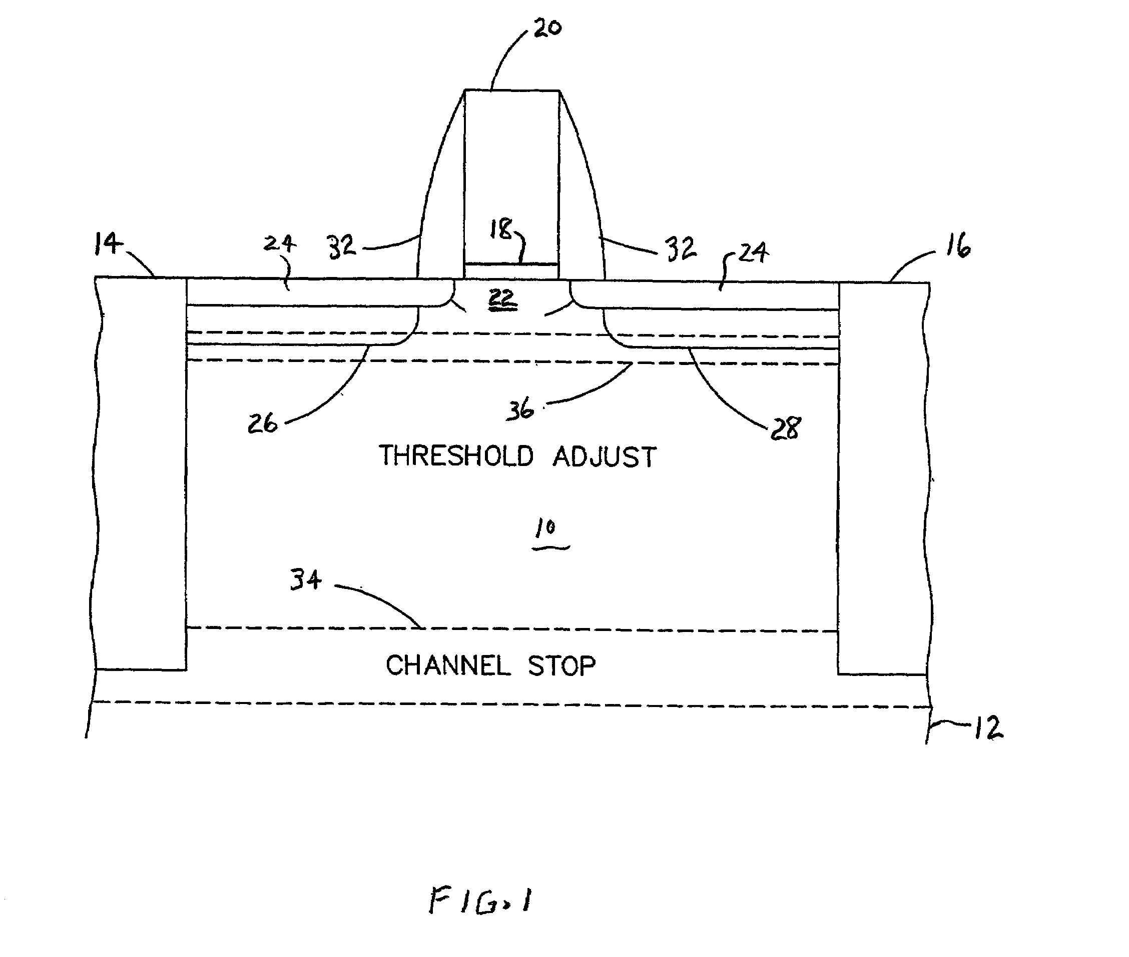
[0018]An enlarged cross-sectional view of an example of an MOS device is shown in FIG. 1. It will be understood that FIG. 1 is simplified and is not drawn to scale. A well 10 (p-well or n-well) is formed in a silicon substrate 12 between isolation regions 14 and 16. A gate electrode 20 is formed over a channel 22. Gate electrode 20 is electrically isolated from channel 22 by a gate dielectric layer 18. Relatively shallow source / drain extensions 24 extend from opposite ends of channel 22 to relatively deep source and drain regions 26 and 28, respectively. A sidewall spacer 32 on the sides of gate electrode 20 facilitates implantation of source and drain regions 26 and 28. The MOS device may further include a channel stop 34 and a threshold adjust 36. A typical CMOS integrated circuit formed on substrate 12 includes multiple n-type MOS devices and multiple p-type MOS devices in a CMOS configuration, as known in the art.

[0019]As noted above, devices with reduced dimensions and increase...


PUM

PropertyMeasurementUnit
thicknessaaaaaaaaaa
thicknessaaaaaaaaaa
thicknessaaaaaaaaaa

Abstract

A method is provided for forming a thin film layer on a substrate. The method includes the steps of doping a thin surface layer on the substrate with low energy ions of a dopant material, and heating the thin surface layer sufficiently to produce a reaction between the dopant material and the surface layer. The heating step is performed simultaneously with at least part of the doping step. The doping step may utilize plasma doping of the thin surface layer. In one embodiment, the doping step includes plasma doping of a silicon oxide layer with nitrogen ions. The heating step may utilize thermal conduction or heating with radiation, such as heating with optical energy. The process may be used for forming dielectric layers having a thickness of 50 angstroms or less.

Description

FIELD OF THE INVENTION [0001]This invention relates to methods for forming thin film layers on substrates, such as semiconductor wafers, and, more particularly, to methods for forming thin film layers by simultaneous doping and sintering. The invention is particularly useful for forming dielectric layers having a thickness of 50 angstroms or less, but is not limited to this application.BACKGROUND OF THE INVENTION [0002]A well-known trend in the semiconductor industry is toward smaller, higher speed devices. In particular, both the lateral dimensions and the depths of features in semiconductor devices are decreasing. State of the art semiconductor devices require junction depths less than 1,000 angstroms and may eventually require junction depths on the order of 200 angstroms or less.[0003]One critical element in the trend toward increased miniaturization is the gate structure of MOS transistors. A dielectric layer overlays the channel, and the gate electrode is disposed on the diele...

Claims


Application Information

Patent Timeline
Patent Type & Authority Patents(United States)
IPC IPC(8): H01L21/469H01L21/31H01L21/265C23C8/80C23C10/02C23C10/60C23C12/02C23C14/48C23C14/58C23C16/56H01L21/28H01L21/314H01L21/316H01L21/318H01L29/51
CPCC23C8/80H01J37/32412C23C10/60C23C12/02C23C14/48C23C14/5806C23C16/56H01L21/28238H01L21/3144H01L21/31604H01L21/28202H01L21/28229C23C10/02H01L21/31612H01L29/517H01L29/518H01L21/265H01L21/0234H01L21/02345
Inventor DOWNEY, DANIEL F.
Owner VARIAN SEMICON EQUIP ASSOC INC
Why Eureka
Try Eureka