

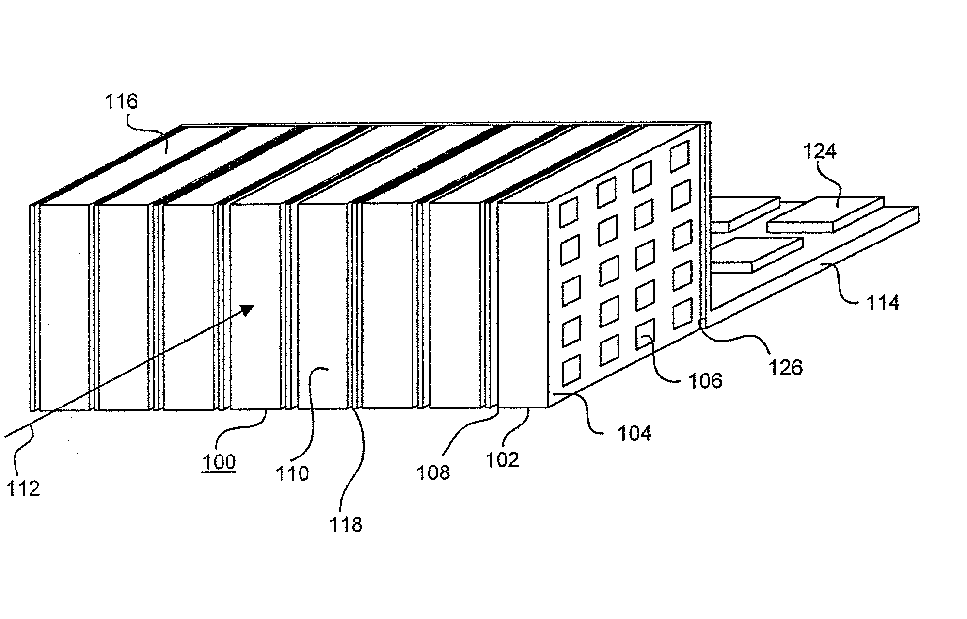
Three dimensional radiation detector
a three-dimensional radiation and detector technology, applied in the field of semiconductor radiation detectors, can solve the problems of high low production yield of such a detector, and the possibility of having defects in the crystal volume from which the detector is sliced, so as to achieve accurate reconstruction of the path of photons and high volume detection utilization of the detector assembly.
- Summary
- Abstract
- Description
- Claims
- Application Information
AI Technical Summary
Benefits of technology
Problems solved by technology
Method used
Image

Examples
Embodiment Construction
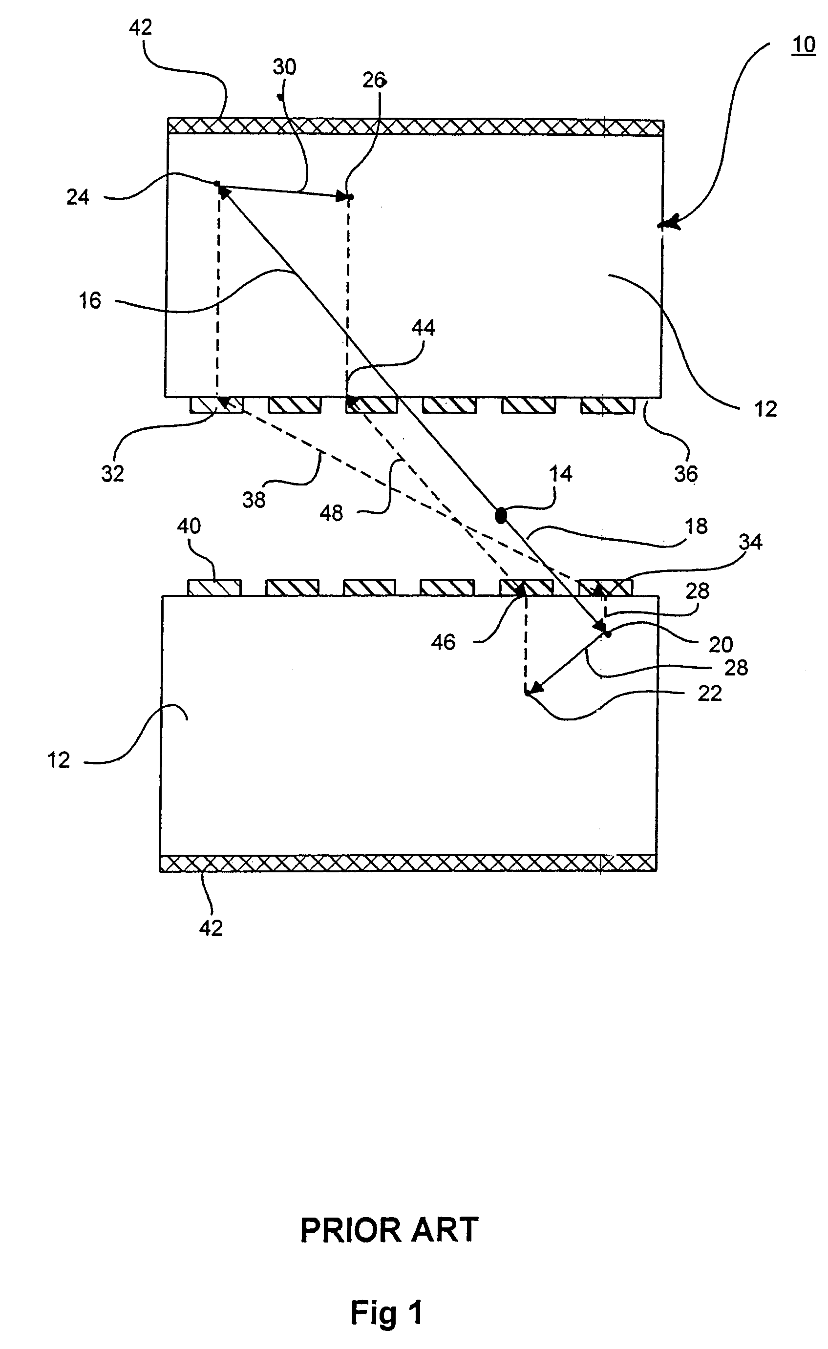
[0026]Reference is now made to FIG. 1, which illustrates schematically a two-headed Gamma ray camera 10 including two identical thick conventional prior art pixelated semiconductor detectors 12, designed to detect high-energy radiation produced by positron emission at point 14, whose location is to be imaged. From point 14 photons 16 and 18 are emitted with the same energy and along oppositely directed directions. Photon 18 might be absorbed at point 20 or alternatively might be scattered by Compton scattering as photon 28 to be absorbed at point 22. Similarly, photon 16 might be absorbed at point 24 or alternatively might be scattered by Compton scattering as photon 30 to be absorbed at point 26.
[0027]The location 14 from which the photons are emitted is derived from the detection location made by detectors 12. For example, in a situation when photons 16 and 18 are absorbed at points 20 and 24, the line on which point 14 is located should be derived by drawing a line that connects ...
PUM
 Abstract
Description
Claims
Application Information