Wiring and method of manufacturing the same, and wiring board and method of manufacturing the same

a wiring board and manufacturing method technology, applied in the direction of transistors, optics, instruments, etc., can solve the problems of reducing the electrical characteristics of the tft, affecting the etching rate of the first layer, so as to achieve the effect of enhancing the etching rate in the first layer

Inactive Publication Date: 2007-01-30
SEMICON ENERGY LAB CO LTD
View PDF49 Cites 35 Cited by
  • Summary
  • Abstract
  • Description
  • Claims
  • Application Information

AI Technical Summary

Benefits of technology

[0012]According to the present invention, wiring has a layered structure that includes: as a first layer, a conductive film mainly containing one or a plurality of kinds of elements selected from W and Mo, or one or a plurality of kinds of elements selected from W and Mo; as a second layer, a low-resistant conductive film mainly containing Al; and as a third layer, a conductive film mainly containing Ti, whereby it is attempted to lower a resistance of wiring. According to the present invention, the low-resistant conductive film mainly containing Al is sandwiched with other conductive films, whereby formation of projections such as hillock and whisker due to a heat treatment can be prevented. Furthermore, since the first and third layers are made of conductive films with a high melting point, they function as barrier metal, which can prevent an Al atom from diffusing to an insulating film and an active region (Table 2). Furthermore, when an insulating film is formed on wiring of the present invention, and contact with the wiring is formed, the third layer functions as a stopper for etching of the insulating film, so that contact can be easily formed. When Al comes into contact with an ITO film (typical transparent conductive film), Al causes electric corrosion to increase a contact resistance. However, the third layer is made of a conductive film mainly containing Ti, so that a contact resistance becomes satisfactory.
[0037]According to the present invention, a low resistance can be realized in wiring by a simple method suitable for processes of manufacturing conventional wiring or wiring board. Therefore, a degree of design freedom and an aperture ratio in a pixel portion can be enhanced. Since wiring includes conductive layers with a taper shape, satisfactory coverage is obtained. Because of such advantages, in a semiconductor device represented by an active matrix type liquid crystal display device, the present invention is fully ready for enlargement of a screen caused by an increased area of a pixel portion, which allows the operation characteristics and reliability of the semiconductor device to be enhanced.

Problems solved by technology

In the case where aluminum (Al) is used as wiring of the above-mentioned TFT in order to manufacture TFT, projections such as hillock and whisker are formed due to a heat treatment, and an Al atom diffuses to an insulating film and an active region (in particular, a channel-formation region), which may cause operation defects of the TFT or a decrease in electrical characteristics of the TFT.
Therefore, when a screen size is enlarged, a wiring delay becomes a problem.
Furthermore, when the film thickness of wiring is made larger, a short-circuit is likely to be caused at a portion where wiring crosses to each other three-dimensionally, and coverage is degraded at the step difference portion of the wiring.

Method used


Image

  • Wiring and method of manufacturing the same, and wiring board and method of manufacturing the same
  • Wiring and method of manufacturing the same, and wiring board and method of manufacturing the same
  • Wiring and method of manufacturing the same, and wiring board and method of manufacturing the same

Examples


embodiment 1

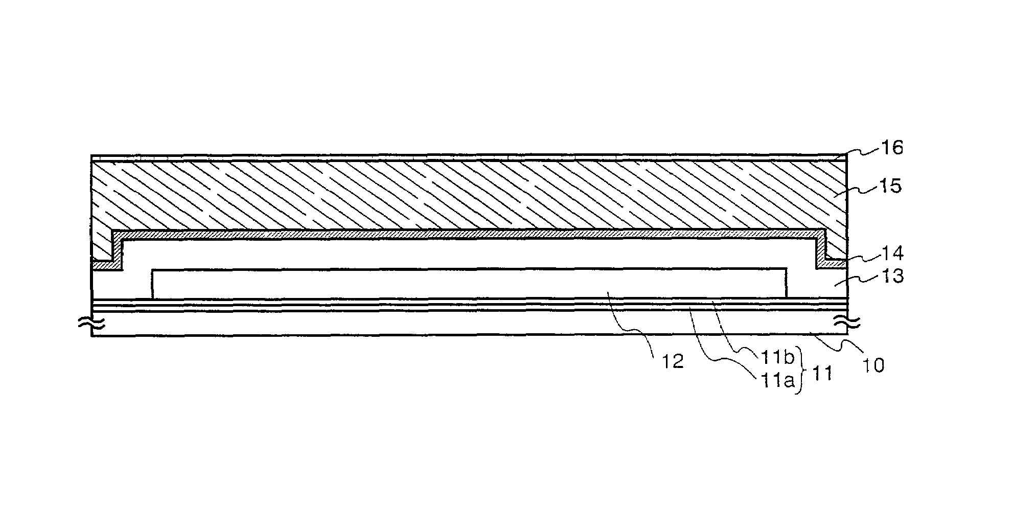
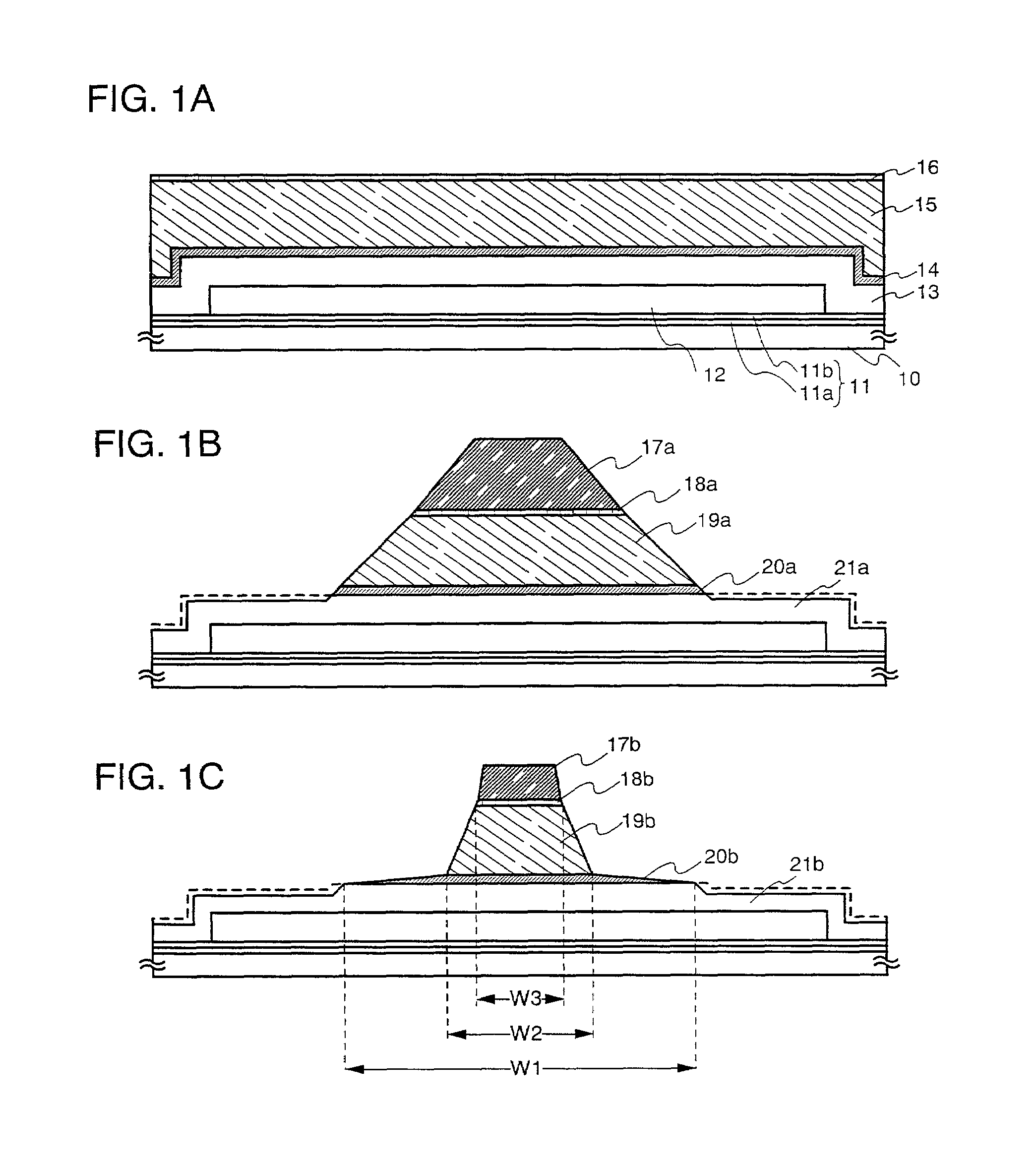
[0074]An exemplary structure of a wiring board provided with a gate electrode using the present invention will be described below.

[0075]First, a base insulating film 11 is formed on a substrate 10. As the substrate 10, a glass substrate, a quartz substrate, a silicon substrate, or a metal substrate or a flexible substrate with an insulating film formed thereon may be used. Furthermore, a plastic substrate having heat resistance withstanding a treatment temperature may be used. In the present embodiment, a glass substrate (1737 produced by Corning Co.) was used.

[0076]As the base insulating film 11, a base film 11 made of an insulating film such as a silicon oxide film, a silicon nitride film, or a silicon oxynitride film is formed. Herein, the base film 11 with a double-layered structure (11a, 11b) is exemplified; however, the base film 11 may be a single-layer film of the insulating film or may have a multi-layered structure of two or more layers. Note that the base insulating film ...

embodiment 2

[0088]In the present embodiment, the case where the first etching condition in the first etching process in Embodiment 1 is changed will be described with reference to FIGS. 3A–3B to 6A–6C. Herein, since the first etching condition is changed, only two layers (second and third conductive layers) in Embodiment 1 constitute a gate line. However, the present invention is also applicable to the case where a gate line is composed of three layers using the first conductive layer in Embodiment 1 as a lower layer.

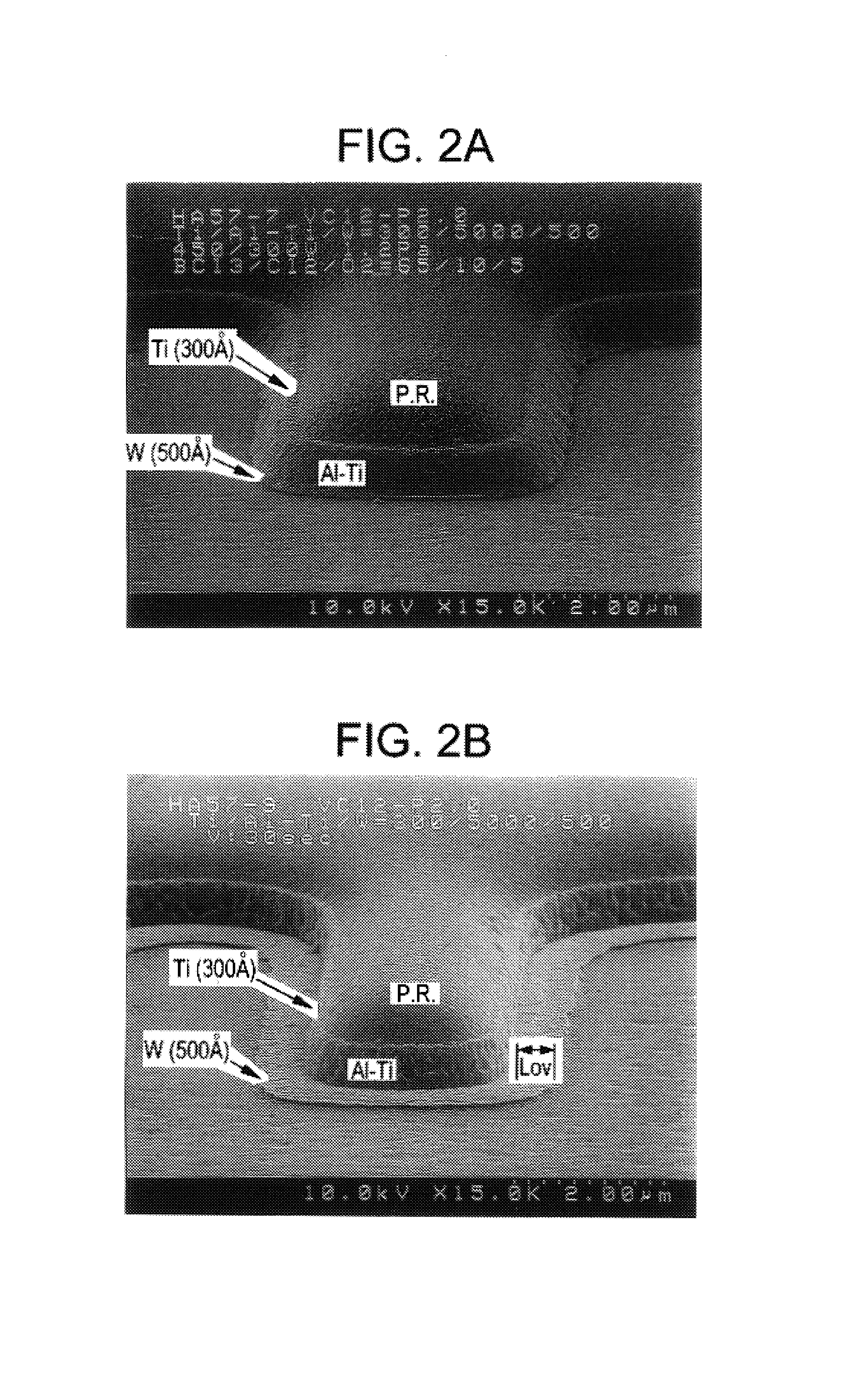
[0089]First, an oxynitride film 33 is formed to have a thickness of 200 nm on a 1737 glass substrate 10 by sputtering. Then, a first conductive film 34 made of an Al—Ti film (thickness: 500 nm) and a second conductive film 35 made of a Ti film (thickness: 100 nm) were layered by sputtering (FIG. 3A).

[0090]Then, an etching process is conducted after forming a resist on the second conductive film 35. This etching process is conducted under the first etching condition in Embodiment 1....

embodiment 3

[0096]In the present embodiment, the case where a plasma treatment is conducted to the wiring formed in Embodiment 1 will be described with reference to FIGS. 17A and 17B. In the present specification, a plasma treatment refers to exposing a sample to an atmosphere in which a gas is subjected to plasma treatment.

[0097]First, in accordance with Embodiment 1, the state shown in FIG. 1C is obtained. FIG. 17A and FIG. 1C show the same state, and corresponding portions are denoted with the same reference numerals.

[0098]The wiring thus formed is subjected to a plasma treatment using oxygen, a gas mainly containing oxygen, or H2O (FIG. 17B). The plasma treatment is conducted for 30 seconds to 20 minutes (preferably, 3 to 15 minutes) using a plasma generating apparatus (plasma CVD apparatus, dry etching apparatus, sputtering apparatus, etc.). Furthermore, it is desirable that the wiring is treated under the condition of a gas flow rate of 50 to 300 sccm, a substrate temperature of room temp...


PUM

PropertyMeasurementUnit
thicknessaaaaaaaaaa
thicknessaaaaaaaaaa
thicknessaaaaaaaaaa

Abstract

The wiring of the present invention has a layered structure that includes a first conductive layer (first layer) having a first width and made of one or a plurality of kinds of elements selected from W and Mo, or an alloy or compound mainly containing the element, a low-resistant second conductive layer (second layer) having a second width smaller than the first width, and made of an alloy or a compound mainly containing Al, and a third conductive layer (third layer) having a third width smaller than the second width, and made of an alloy or compound mainly containing Ti. With this constitution, the present invention is fully ready for enlargement of a pixel portion. At least edges of the second conductive layer have a taper-shaped cross-section. Because of this shape, satisfactory coverage can be obtained.

Description

BACKGROUND OF THE INVENTION[0001]1. Field of the Invention[0002]The present invention relates to wiring formed by using a thin film technique and a method of manufacturing the same. The present invention also relates to a wiring board and a method of manufacturing the same. In the present specification, a wiring board refers to an insulating substrate made of glass, etc. or various substrates having wiring formed by using a thin film technique.[0003]2. Description of the Related Art[0004]In recent years, a technique of forming a thin film transistor (TFT) using a semiconductor thin film (thickness of about several to hundreds of nm) formed on a substrate with an insulating surface has been paid attention to. A TFT is widely applied to an electronic device such as an integrated circuit (IC) and an electrooptic apparatus. In particular, a TFT is being rapidly developed as a switching element of an image display apparatus.[0005]Conventionally, a liquid crystal display device as an imag...

Claims


Application Information

Patent Timeline
Patent Type & Authority Patents(United States)
IPC IPC(8): H01L21/461H01L21/302G02F1/1345G02F1/1362H01L21/336H01L23/528H01L23/532H01L27/32H01L29/786H01L51/52
CPCH01L23/5283H01L23/53223H01L29/4908H01L29/66757H01L29/78621H01L29/78645H01L29/78648G02F2001/13629H01L2924/0002H01L27/3241H01L51/5203H01L2924/12044H01L2924/3011H01L2924/00G02F1/13629H10K59/10H10K59/805G02F1/1345H10K50/805
Inventor YAMAZAKI, SHUNPEISUZAWA, HIDEOMIONO, KOJIKUSUYAMA, YOSHIHIRO
Owner SEMICON ENERGY LAB CO LTD
Why Eureka
Try Eureka