Methods of hyperdoping semiconductor materials and hyperdoped semiconductor materials and devices

a technology of semiconductor materials and materials, applied in the direction of polycrystalline material growth, crystal growth process, chemically reactive gas, etc., can solve the problems of limiting device performance and reliability, counterproductive side effects, and failure to raise the maximum practical carrier concentration of matrix materials

Inactive Publication Date: 2007-02-20
YALE UNIV
View PDF13 Cites 33 Cited by
  • Summary
  • Abstract
  • Description
  • Claims
  • Application Information

AI Technical Summary

Benefits of technology

[0018]Yet another object of the invention relates to methods for creating a semiconductor material including one or more dopants, while avoiding or mitigating the formation of one or more of the following effects ordinarily found at the doping level of said materials formed by prior art methods: (i) precipitation of the dopant; (ii) interstitial dopant; (iii) anti-site or vacancy compensation of the dopant; (iv) migration of a dopant; (v) amphoteric dopant compensation and / or (vi) non-radiative recombination centers.
[0023]Another object of the invention relates to processes for manufacturing semiconductor devices with superior operating properties, such as: (a) higher operating speed; (b) lower RC time constants; (c) greater power efficiency or lower power losses; (d) better heat sinking; (e) higher duty cycle; (f) lower threshold voltage; (g) superior operating voltage (h) lower threshold current; (i) higher gain; (j) higher stability; (k) higher radiometric efficiency; (l) higher quantum efficiency; (m) higher photometric efficiency; (n) higher brightness; (o) faster electro-luminescent modulation; (p) higher relaxation oscillation frequency; (q) lower relative intensity noise; (r) lower wavelength spread (breadth or narrowness); (s) optimized wavelength centroid; and / or (t) improved device-to-device reproducibility. Yet another object of the invention relates to processes for manufacturing improved-performance heterojunction bipolar transistors (HBTs) or similar devices with (i) relatively thinner base regions, (ii) higher base-region doping and / or (iii) lower extrinsic base resistance. Yet another object of the invention is to provide for a reduction in the surface recombination rate through the use of hyperdoped semiconductor material.
[0025]Still another object of the invention is to provide for a layer of semiconductor material having an electric field established through the layer by the use of hyperdoped semiconductor material to provide a doping gradient. A still further object of the invention is to provide for reduced device bulk resistance(s) through the use of hyperdoped semiconductor material.
[0030]Growing hyperdoped semiconductor materials in a substantially oxygen-free environment may involve maintaining a partial pressure of less than 10−9 torr, and advantageously a partial pressure of less than 10−10 torr, and preferably a partial pressure of less than 10−11 torr, for oxygen atoms, oxygen molecules and oxygen radicals, as well as oxygen-containing compounds such as, but not limited to, water, oxides of gallium (e.g. from a Ga effusion cell or otherwise), arsenic oxide (e.g. from a arsenic effusion cell or otherwise) and dopant oxides. Growing hyperdoped semiconductor materials in a substantially oxygen-free environment may also involve maintaining partial pressures of oxygen-based contaminants that are sufficiently low to avoid substantial degradation of the hyperdoped semiconductor materials' electroluminescence and / or sufficiently low to avoid substantial formation of performance degrading non-radiative recombination channels in the hyperdoped semiconductor materials.

Problems solved by technology

Also well known in the art is the fact that for various host materials (also referred to herein as matrix materials) under given growth conditions, there will be a saturation limit for the carrier concentration produced by a dopant, and attempts to increase the dopant concentration beyond this limit will generally fail to raise the maximum practical carrier concentration in the matrix material, or even without apparent carrier saturation may produce counterproductive side effects.
These side effects include degraded minority carrier lifetimes and enhanced dopant diffusion, which often limit device performance and reliability.
Prior art methods cannot effectively dope near or beyond the carrier saturation limit because dopant concentrations near or beyond the carrier saturation limit behave differently in the crystal lattice compared to the dopant at lower concentrations.
These compensating mechanisms generally tend to result in an increase in the non-radiative trap density.
Minority carrier lifetime is reduced in the presence of such non-radiative traps, resulting in the reduction of the efficiency of minority carrier devices.
Shortened minority carrier lifetimes also diminish bipolar transistor gain, β. Non-radiative recombination has also been linked to performance degradation over time, leading to reliability concerns.
For example, interstitial atoms provide both a non-radiative recombination site and tend to diffuse rapidly at elevated temperatures or in the presence of high-electrical fields, aging the material and causing performance degradation and failures.
For example, interstitial Be dopant atoms in the base of a npn heterojunction bipolar transistor (HBT) tend to rapidly diffuse into the emitter, especially at elevated temperatures and under current stressing, irreversibly degrading the performance of the HBT.
), and experiments with heavily C-doped LEDs demonstrated a high cutoff frequencies but unacceptably low internal (hence, low external) quantum efficiencies for light-emitting applications, indicating a serious increase in the non-radiative recombination rate.
Be dopant atoms, since they become interstitial much more readily than C dopant atoms, therefore migrate much more readily than C, and are comparatively unstable.
There are, however, critical limitations for C doping.
Doping C to a concentration above this amount can lead to formation of precipitates, which are known to degrade HBT performance.
Non-radiative recombination greatly degrades electroluminescence, as well as limiting HBT transistor gain to unacceptably low values.
Additionally, p-type C doping is technologically more difficult for In-based III-V compounds and their alloys, e.g., InP and InGaAs.

Method used


Image

  • Methods of hyperdoping semiconductor materials and hyperdoped semiconductor materials and devices
  • Methods of hyperdoping semiconductor materials and hyperdoped semiconductor materials and devices
  • Methods of hyperdoping semiconductor materials and hyperdoped semiconductor materials and devices

Examples


Embodiment Construction

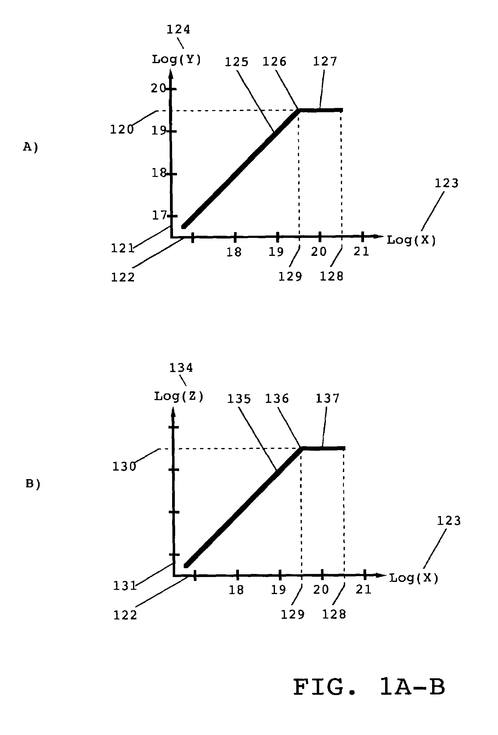
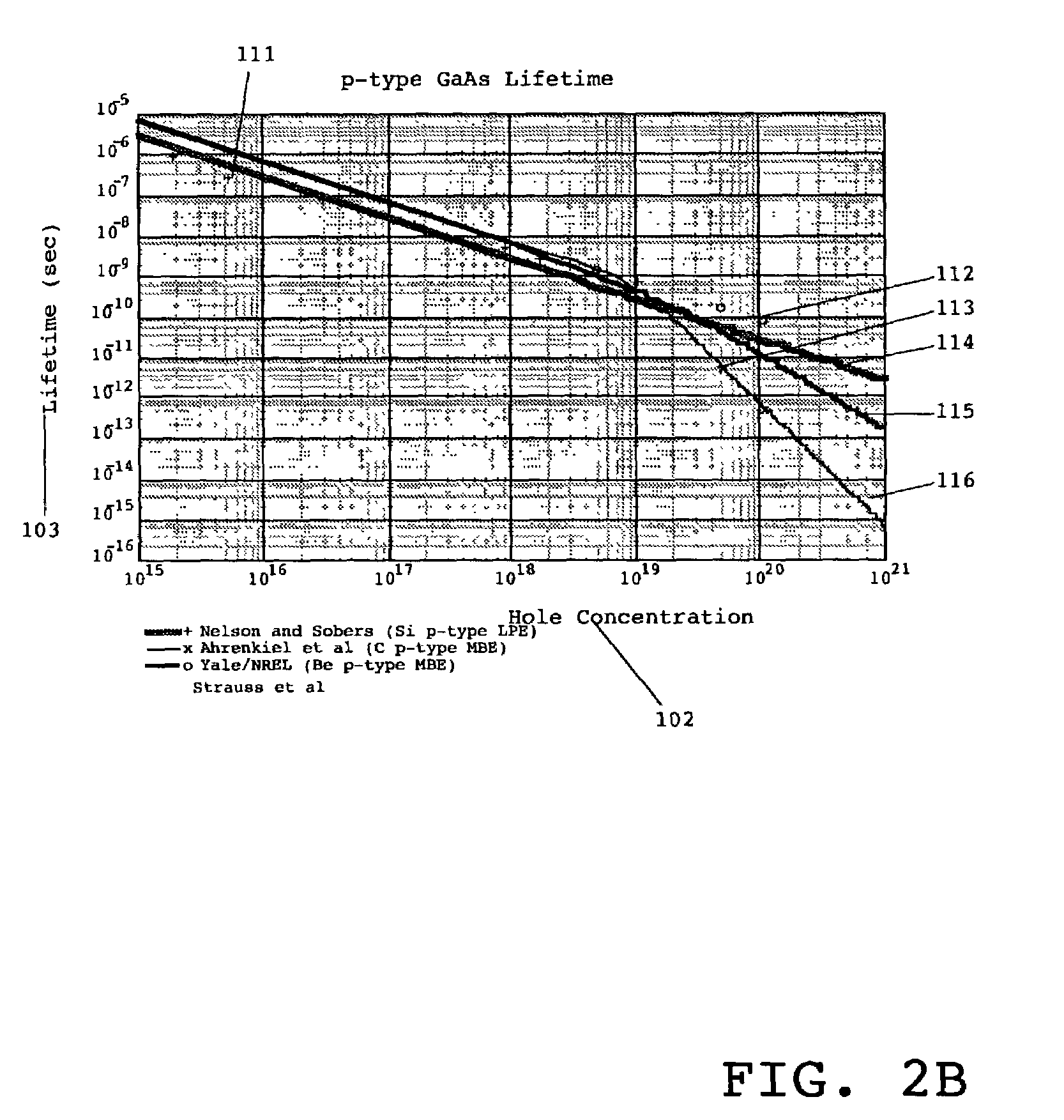
[0054]As employed herein, a hyperdoped compound semiconductor material is a material having a suitable excess anion (cation) pressure incorporated into the matrix such that, compared to prior art materials, nearly all of the dopant atoms occupy cation (anion) sites, so that compensating effects such as interstitial dopants, amphotericity, crystalline defects such as anti-site or vacancy defects, dopant precipitation, or co-incorporation of contaminating species such as oxygen are greatly reduced. In a preferred, but not limiting embodiment on crystals containing GaAs, a process of hyperdoping involves creating an excess anion concentration (e.g., an excess As concentration) and permits the forcing of Be onto cation sites (e.g. Ga sites), without introducing a significant density of non-radiative recombination centers. Hyperdoping may be used to create materials with reduced radiative lifetime (because radiative lifetime is approximately proportional to doping density, higher doping ...


PUM

PropertyMeasurementUnit
hole concentrationaaaaaaaaaa
temperaturesaaaaaaaaaa

Abstract

Methods are disclosed for producing highly doped semiconductor materials. Using the invention, one can achieve doping densities that exceed traditional, established carrier saturation limits without deleterious side effects. Additionally, highly doped semiconductor materials are disclosed, as well as improved electronic and optoelectronic devices / components using said materials. The innovative materials and processes enabled by the invention yield significant performance improvements and / or cost reductions for a wide variety of semiconductor-based microelectronic and optoelectronic devices / systems.Materials are grown in an anion-rich environment, which, in the preferred embodiment, are produced by moderate substrate temperatures during growth in an oxygen-poor environment. The materials exhibit fewer non-radiative recombination centers at higher doping concentrations than prior art materials, and the highly doped state of matter can exhibit a minority carrier lifetime dominated by radiative recombination at higher doping levels and higher majority carrier concentrations than achieved in prior art materials. Important applications enabled by these novel materials include high performance electronic or optoelectronic devices, which can be smaller and faster, yet still capture or emit light efficiently, and high performance electronics, such as transistors, which can be smaller and faster, yet cooler.

Description

CROSS-REFERENCE TO RELATED APPLICATION[0001]This application claims priority from U.S. Provisional Patent Applications 60 / 341,051 (filed Oct. 22, 2001) and 60 / 350,503 (filed Jan. 22, 2002), both of which are incorporated by reference herein.FIELD OF THE INVENTION[0002]This invention relates generally to the fields of solid-state physics and electronics, more particularly to the design and fabrication of semiconductor materials and devices, and still more particularly to the design and fabrication of semiconductor materials and devices for high-performance optoelectronic and microelectronic applications.BACKGROUND OF THE INVENTION[0003]Molecular beam epitaxy (MBE) is a well known and widely used technique for building semiconductor (or other) materials on a substrate. Typically, MBE directs neutral beams of molecules at a target substrate, while maintaining process conditions (e.g., substrate temperature, etc.) and stoichiometry that encourage growth of the desired material (typicall...

Claims


Application Information

Patent Timeline
Patent Type & Authority Patents(United States)
IPC IPC(8): C30B9/00C30B23/02C30B25/02H01L21/203H01L21/331H01L21/335H01L21/337H01L21/338H01L29/207H01L29/36H01L29/737H01L29/778H01L29/80H01L29/812H01L33/02
CPCC30B23/02H01L33/025C30B29/40C30B29/403C30B29/406H01L21/02395H01L21/02538H01L21/02546H01L21/02573H01L21/02579H01L21/02631H01L29/207H01L29/36H01L29/66318H01L29/66462H01L29/66924H01L29/7371H01L29/7785H01L29/802C30B25/02
Inventor BOONE, THOMASHARMON, ERIC S.KOUDELKA, ROBERT D.SALZMAN, DAVID B.WOODALL, JERRY M.
Owner YALE UNIV
Why Eureka
Try Eureka