Ultraviolet sensor and method for manufacturing the same

a technology of ultraviolet light and sensors, applied in the field of ultraviolet light sensors, can solve the problems of reducing electrical resistance, decomposition of organic compounds present in the atmosphere, dissociation of moisture adsorbed on the sensor surface into ions, etc., and achieves the effect of preventing the adhesion of moisture, constant responsibility, and preventing moisture and organic compounds

Inactive Publication Date: 2007-03-20
KOBE STEEL LTD
View PDF4 Cites 53 Cited by
  • Summary
  • Abstract
  • Description
  • Claims
  • Application Information

AI Technical Summary

Benefits of technology

[0013]The present invention has been made to solve the above problems. It is an object of the present invention to provide an ultraviolet sensor, manufactured with low cost, having a constant responsivity that does not change for a long time and also provide a method for manufacturing the ultraviolet sensor.
[0016]In order to achieve the above object, the inventors have performed an intensive investigation and then found that when an exposed section of the diamond layer is covered with an oxide layer or a fluoride layer, moisture and organic compounds hardly adhere to the covered section and the sensor therefore has a constant responsibility. In the present invention, the oxide layer or the fluoride layer is placed on the sub-region of the detecting region that is not covered with the electrodes. Therefore, moisture and organic compounds can be prevented from adhering to the exposed section of the diamond layer.
[0017]The oxide layer preferably contains at least one selected from the group consisting of alumina, silica, titania, and zirconia. The fluoride layer preferably contains at least one of calcium fluoride and magnesium fluoride. This prevents the adhesion of moisture and organic compounds without causing a deterioration in electric properties of the diamond layer and the ultraviolet transmittance thereof.
[0018]In the ultraviolet sensor, the diamond layer preferably has a (100) surface and crystal grains which are arranged at the (100) surface, which are oriented in a single direction, and of which the in-plane directions are aligned with each other. Such a layer is known to a highly oriented diamond layer and is herein defined as a layer, made of polycrystalline diamond, having crystal grains of which the growth directions are aligned with each other and of which the in-plane directions are also aligned with each other. The diamond layer has a characteristic surface at which smooth (001) facets are arranged. Therefore, the diamond layer has a smaller number of crystal defects present at the surface thereof as compared to ordinary polycrystalline layers; hence, the diamond layer has a carrier mobility that is one order greater than that of known one. Thus, the ultraviolet sensor has higher detection performance as compared to known ultraviolet sensors.
[0019]In a method for manufacturing the ultraviolet sensor according to the present invention, the covering layer may be formed by, for example, a sputtering process, a vapor deposition process, a laser ablation process, or a chemical vapor deposition process. Alternatively, the covering layer may be formed by a process including a vacuum process. This leads to the stability of the ultraviolet sensor. The diamond layer is preferably polycrystalline formed by a vapor growth process. This allows the diamond layer, which is highly controllable, to be readily manufactured.
[0020]According to the present invention, since moisture and organic compounds can be prevented from adhering to the exposed region of the diamond layer, the diamond layer is allowed to have constant responsivity without causing a deterioration in the ultraviolet transmittance and electrical properties of the diamond layer.

Problems solved by technology

The first problem is that organic compounds present in an atmosphere are decomposed during the irradiation because of the high energy of the short-wavelength light and the decomposed products adhere to the surfaces of the sensors.
The second problem is that moisture adsorbed on the sensor surfaces is dissociated into ions if the moisture is irradiated with strong ultraviolet light.
Such ions cause a decrease in electrical resistance because they are caused to migrate on the sensor surfaces readily and slowly by an electric field applied between the electrodes.
In this case, since the output of the sensors varies over several hundred seconds at the start or end of the ultraviolet irradiation, an output corresponding to the intensity of light cannot be obtained.
However, the use of such a sealed package causes an increase in the number of manufacturing steps and an increase in the number of optical components and this causes an increase in manufacturing cost.
Furthermore, since it is substantially impossible to completely remove moisture and organic compounds adsorbed on the inner surface of the package in advance, the moisture and the organic compounds remain semi-permanently in the package to cause contamination in the package and this causes a deterioration in properties in some cases.
However, such a Schottky or pn junction cannot be substantially formed in any diamond film; hence, no photodiode-type sensor including any diamond film can be used.
However, there is a problem in that the vertical ultraviolet sensor 104 has unsatisfactory properties because the polycrystalline diamond layer 102 has a high density of grain boundaries present close to the conductive substrate 105 and therefore has a high density of crystal defects if the polycrystalline diamond layer 102 is formed by a vapor deposition process.
The crystal defect density can be reduced by increasing the thickness of the polycrystalline diamond layer 102 and polishing the rear face thereof; however, this technique causes a serious increase in manufacturing cost and cannot therefore be applied to a sensor for mass production.
Furthermore, there is a problem in that the vertical ultraviolet sensor 104 has low detection efficiency because the electrode 106 lies over the polycrystalline diamond layer 102 functioning as a detector and reflects or absorbs ultraviolet light.

Method used


Image

  • Ultraviolet sensor and method for manufacturing the same
  • Ultraviolet sensor and method for manufacturing the same
  • Ultraviolet sensor and method for manufacturing the same

Examples


examples

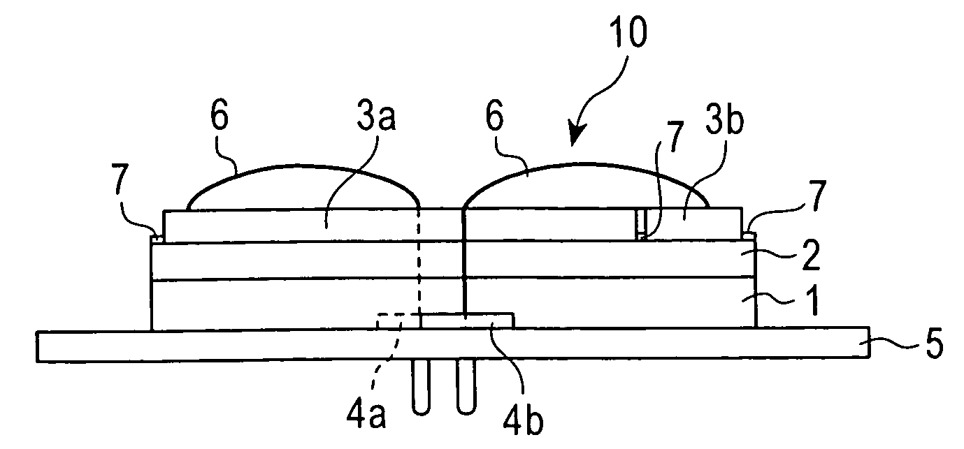
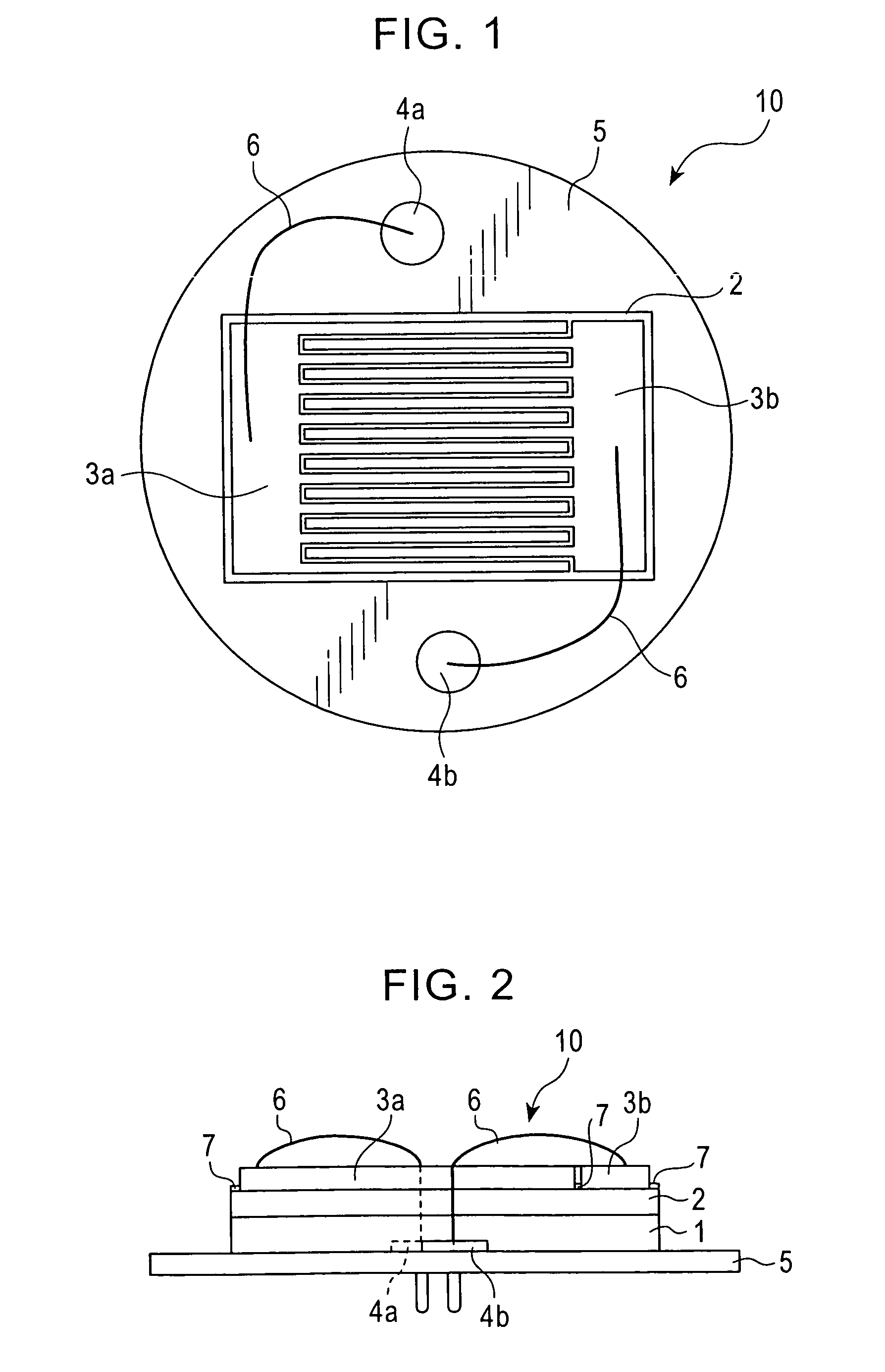
[0040]Ultraviolet sensors having the same configuration as that of the ultraviolet sensor 10 shown in FIG. 2 were prepared by the procedure below and then used as samples of an example of the present invention. A (001) silicon wafer 1 with low resistivity was prepared and then exposed to a mixture of methane plasma and hydrogen plasma, whereby the wafer surface was carbonized. A bias voltage was applied to the resulting wafer 1 in the mixture of methane plasma and hydrogen plasma, whereby diamond nuclei were formed on the wafer 1 by epitaxial growth. The application of the bias voltage to the wafer 1 was stopped and diamond was deposited on the wafer 1 for 15 hours using a gas mixture of methane and hydrogen under such conditions that a (100) diamond surface was primarily formed, whereby a highly-oriented insulating diamond layer 2 was formed on the wafer 1. The insulating diamond layer 2 had a (100) surface and a thickness of about 10 μm and crystal grains thereof were oriented in ...


PUM

PropertyMeasurementUnit
wavelengthaaaaaaaaaa
thicknessaaaaaaaaaa
thicknessaaaaaaaaaa

Abstract

An ultraviolet sensor includes a substrate; a diamond layer, placed on the substrate, functioning as a detector; and at least one pair of surface electrodes arranged on the diamond layer. The diamond layer has a detecting region present at the surface thereof, the detecting region has at least one sub-region exposed from the surface electrodes, and the sub-region has a covering layer, made of oxide or fluoride, lying thereon. A method for manufacturing the ultraviolet sensor includes a step of forming a diamond layer, functioning as a detector, on a substrate; a step of forming at least one pair of surface electrodes on the diamond layer; and a step of forming a covering layer, made of oxide or fluoride, on at least one sub-region of a detecting region present at the surface of the diamond layer, the sub-region being exposed from the surface electrodes.

Description

BACKGROUND OF THE INVENTION[0001]1. Field of the Invention[0002]The present invention relates to ultraviolet sensors, including diamond films, for detecting ultraviolet light without being affected by solar light and also relates to method for manufacturing such sensors. The present invention particularly relates to an ultraviolet sensor including a highly oriented diamond film and a method for manufacturing such a sensor.[0003]2. Description of the Related Art[0004]In recent years, various ultraviolet sensors have been proposed (see, for example, Japanese Unexamined Patent Application Publication Nos. 5-335613 and 11-248531; UV Photodetectors from Thin Film Diamond; Phys. Stat. Sol. (a), 1996, vol. 154, pp. 445–454; Diamond UV photodetectors: sensitivity and speed for visible blind applications; Diamond and Related Materials, 1998, vol. 7, pp. 513–518; Polycrystalline diamond photoconductive device with high UV-visible discrimination; and Appl. Phys. Lett., 1995, vol. 67, pp. 2117–...

Claims


Application Information

Patent Timeline
Patent Type & Authority Patents(United States)
IPC IPC(8): H01L29/15H01L31/00H01L31/08G01J1/02G01J1/42H01L31/101
CPCG01J1/429H01L31/028H01L31/09H01L31/1085G01J2001/0276Y02E10/547H01L2224/45144H01L2224/48091H01L2924/10253H01L2924/00014H01L2924/00H01L2924/12032G01J1/02G01J1/42
Inventor HAYASHI, KAZUSHITACHIBANA, TAKESHIYOKOTA, YOSHIHIROKAWAKAMI, NOBUYUKI
Owner KOBE STEEL LTD
Why Eureka
Try Eureka