Gradient structures interfacing microfluidics and nanofluidics, methods for fabrication and uses thereof

a technology of nanofluidics and nanofluidics, applied in the field of bionanotechnology, can solve the problems of affecting the performance of conventional nanofluidic devices, unfavorable spontaneous elongation of long biopolymers, and difficulty in efficiently moving, so as to reduce the local entropic barrier and achieve high throughput

Active Publication Date: 2007-05-15
PRINCETON UNIV
View PDF46 Cites 142 Cited by
  • Summary
  • Abstract
  • Description
  • Claims
  • Application Information

AI Technical Summary

Benefits of technology

[0012]The present invention relates to a device for interfacing nanofluidic and microfluidic components suitable for use in performing high throughput i.e., macromolecular analysis. Diffraction gradient lithography (DGL) is used to form a gradient interface between a microfluidic area and a nanofluidic area. The gradient interface area reduces the local entropic barrier to nanochannels formed in the nanofluidic area.

Problems solved by technology

It is challenging to efficiently move long DNA arranged as a blob into the small channels, since it is energetically unfavorable for long biopolymers to spontaneously elongate and enter nanochannels directly from the environment due to the large free energy needed to overcome negative entropy change, as illustrated in FIGS. 1A–1B.
Consequently, problems such as DNA clogging at the junction of nano- and macro-environment have arisen and undermine the performance of conventional nanofluidic devices.
Steps needed in removing the sacrificial materials, such as heating the substrate up to 200–400° C., limits the use of certain materials.
Electron beam lithography has the flexibility to write different patterns, but has low throughput and high manufacturing costs.

Method used


Image

  • Gradient structures interfacing microfluidics and nanofluidics, methods for fabrication and uses thereof
  • Gradient structures interfacing microfluidics and nanofluidics, methods for fabrication and uses thereof
  • Gradient structures interfacing microfluidics and nanofluidics, methods for fabrication and uses thereof

Examples


examples

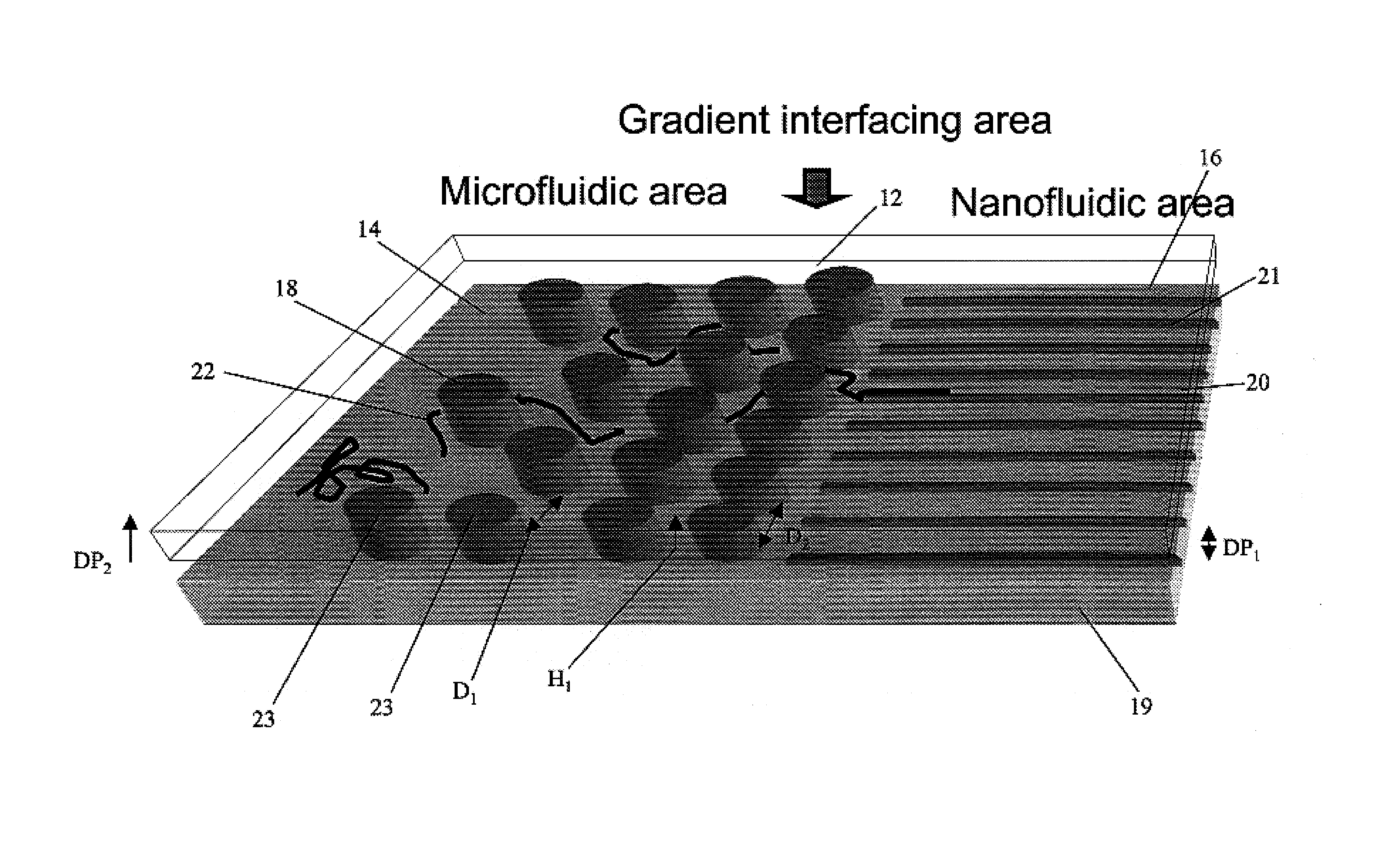
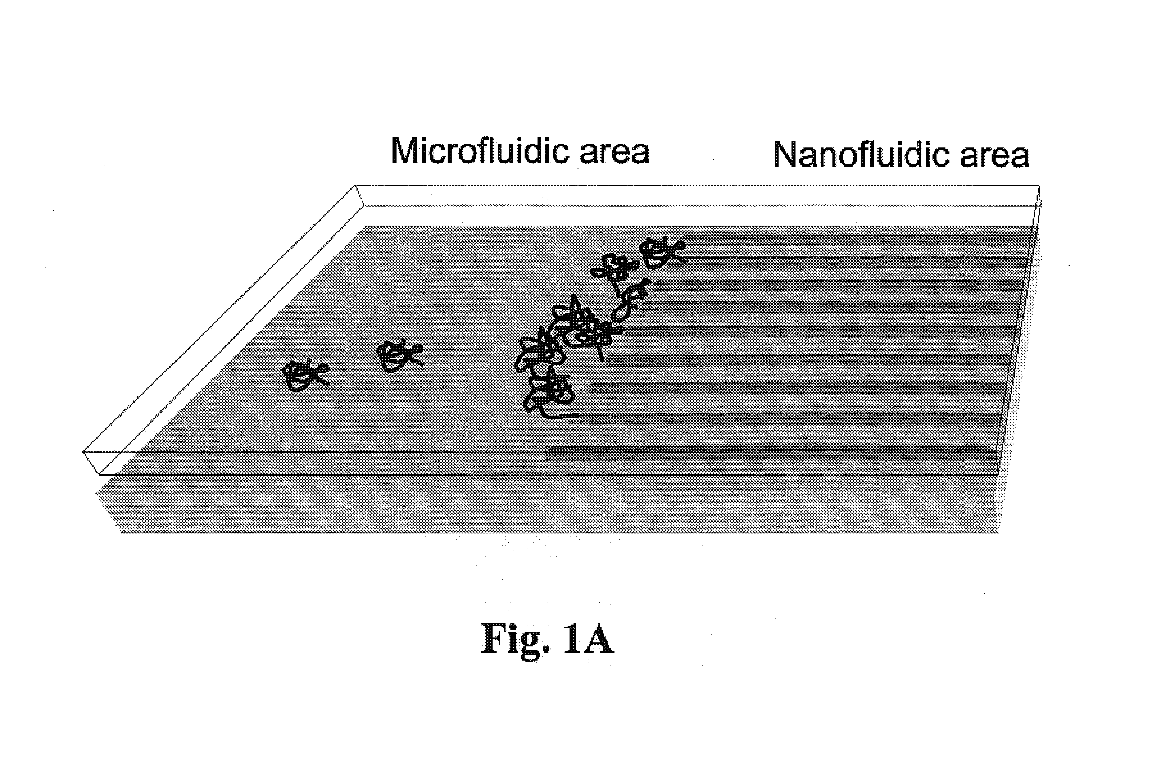
[0079]Large arrays of nanochannels were first fabricated on an entire Si substrate chip using nanoimprinting lithography, described in S. Y. Chou, P. R. Krauss, and P. J. Renstrom, Appl. Phys. Lett. 67 (21), 3114 (1995); Stephen Y. Chou, Peter R. Krauss and Preston J. Renstrom, Science 272, 85 (1996) and U.S. Pat. No. 5,772,905. This chip was spin coated with positive tone photoresist (AZ5214-E) using standard protocol at 4000 rpm for 1 min after HMDS treatment and baked at 110° C. for 2 min. A Karl Suss MA-6 contact aligner and a uniform micron feature size hexagon array photomask were used to pattern the microfluidic area. A blocking mask of a piece of aluminum foil was placed on top of the photomask. The distance between the blocking mask and the photoresist surface was about 3 mm. The chip was exposed at 400 nm UV light in hard contact mode for 35 seconds and developed with a standard procedure (AZ312 MIF:H2O 1:1). The photoresist was used as an etching mask during a subsequent ...


PUM

PropertyMeasurementUnit
distanceaaaaaaaaaa
lateral spacing distanceaaaaaaaaaa
distanceaaaaaaaaaa

Abstract

The present invention relates to a device for interfacing nanofluidic and microfluidic components suitable for use in performing high throughput macromolecular analysis. Diffraction gradient lithography (DGL) is used to form a gradient interface between a microfluidic area and a nanofluidic area. The gradient interface area reduces the local entropic barrier to nanochannels formed in the nanofluidic area. In one embodiment, the gradient interface area is formed of lateral spatial gradient structures for narrowing the cross section of a value from the micron to the nanometer length scale. In another embodiment, the gradient interface area is formed of a vertical sloped gradient structure. Additionally, the gradient structure can provide both a lateral and vertical gradient.

Description

[0001]This patent application claims the benefit of priority to U.S. Provisional Patent Application No. 60 / 373,409, filed on Apr. 16, 2002 and U.S. Provisional Patent Application No. 60 / 419,742, filed Oct. 18, 2002.[0002]DARPA Grant Number MDA972-00-1-0031 supported work that led to portions of the inventions described herein. Accordingly, the U.S. Government may have rights in these inventions.BACKGROUND OF THE INVENTION[0003]1. Field of the Invention[0004]The present invention relates to bionanotechnology and in particular to a method of fabricating a hybrid microfluidic / nanofluidic device having a gradient structure formed by a modified photolithography technique at the interface between microfluidic and nanofluidic portions of the device and uses thereof.[0005]2. Description of the Related Art[0006]Nanotechnology, electronics and biology are combined in the newly emerging field of bionanotechnology. Nanofabrication of extremely small fluidic structures, such as channels, can be ...

Claims


Application Information

Patent Timeline
Patent Type & Authority Patents(United States)
IPC IPC(8): C12M3/00C12Q1/68G01N15/06C07H21/04G01N37/00B01J19/00B01L3/00B81B1/00B82B3/00C12M1/00C12N15/09G03F7/20
CPCB01L3/502707B01L3/502746B01L3/502761B81C1/00119B82Y30/00G01N33/48721G03F7/2008G01N21/6486Y10T436/143333B01L2200/027B01L2200/0663B01L2200/12B01L2300/0654B01L2300/0896B01L2400/0415B01L2400/086B81B2201/058B81C2201/0157B81C2201/0159B01L3/502715
Inventor CAO, HANTEGENFELDT, JONAS O.CHOU, STEPHENAUSTIN, ROBERT H.
Owner PRINCETON UNIV
Why Eureka
Try Eureka