Low-K gate spacers by fluorine implantation

Active Publication Date: 2007-06-05
GLOBALFOUNDRIES US INC
View PDF17 Cites 22 Cited by
  • Summary
  • Abstract
  • Description
  • Claims
  • Application Information

AI Technical Summary

Benefits of technology

[0009]The low-K dielectric gate sidewall spacers result in reduced capacitance through the gate sidewall spacer. By appropriate selection of the fluorine implant dosage and energy, the dielectric constant of the gate dielectric in the gate-to-diffusion overlap region is also reduced, thereby reducing the overlap capacitance and the GIDL field in the Si at the drain diffusion. Furthermore, the reliability of the gate dielectric, partic

Problems solved by technology

Device feature scaling has associated fundamental problems

Method used


Image

  • Low-K gate spacers by fluorine implantation
  • Low-K gate spacers by fluorine implantation
  • Low-K gate spacers by fluorine implantation

Examples


Example

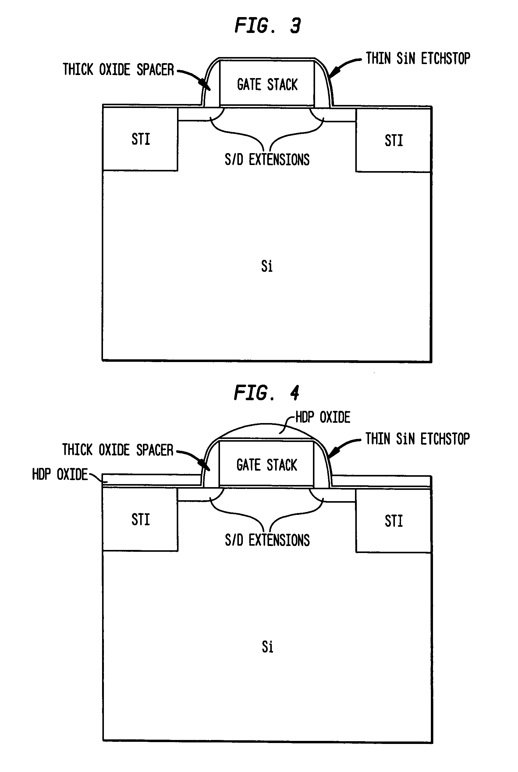
[0022]In a first embodiment, standard gate sidewall CVD oxide spacers are formed by CVD (chemical vapor deposition) and RIE (reactive ion etching), and then a thin silicon nitride etch stop barrier and an HDP (high density plasma) oxide layer are deposited. The HDP oxide deposits primarily on the horizontal surfaces. Then an angled (10 to 90 degrees with 45 degrees being preferred) fluorine implant is performed into the spacers. The angled fluorine implant penetrates the thin nitride layer and is deposited into the thick oxide spacers.

[0023]The fluorine is used to lower the dielectric constant of the spacers, thus reducing the gate to stud capacitance and the gate to diffusion capacitance. In this embodiment, the fluorine only penetrates the spacer, not the gate dielectric. Since the fluorine diffuses rapidly into the spacers and more slowly in a nitridized gate oxide, the dielectric constant of the gate sidewall spacers increases the Teff (effective thickness) of the gate insulator...

Example

[0028]In a second embodiment, the F implant dosage and energy range (F dosage range=1E14 to 2E16 cm-2 with 2E15 cm-2 being preferred, implant energy=5 to 100 keV with 50 keV being preferred) is precisely set to influence the junction / contact region. This will locally alter the gate dielectric characteristic, increasing the threshold voltage of the device. This technique reduces the halo dose requirement, and will also decrease the perimeter capacitance of the device. The penalty for this action is an increase in sub-threshold swing, but this can be compensated by adjusting the threshold voltage.

[0029]Another benefit of this method (over a bird's beak for example) is reduced stress and reduced dislocations in the silicon, which minimizes junction leakage currents. Such a device design is favorable for a DRAM transfer device.

[0030]For both device descriptions discussed, the gate electric field is reduced in the silicon, and the GIDL junction leakage current is also reduced.
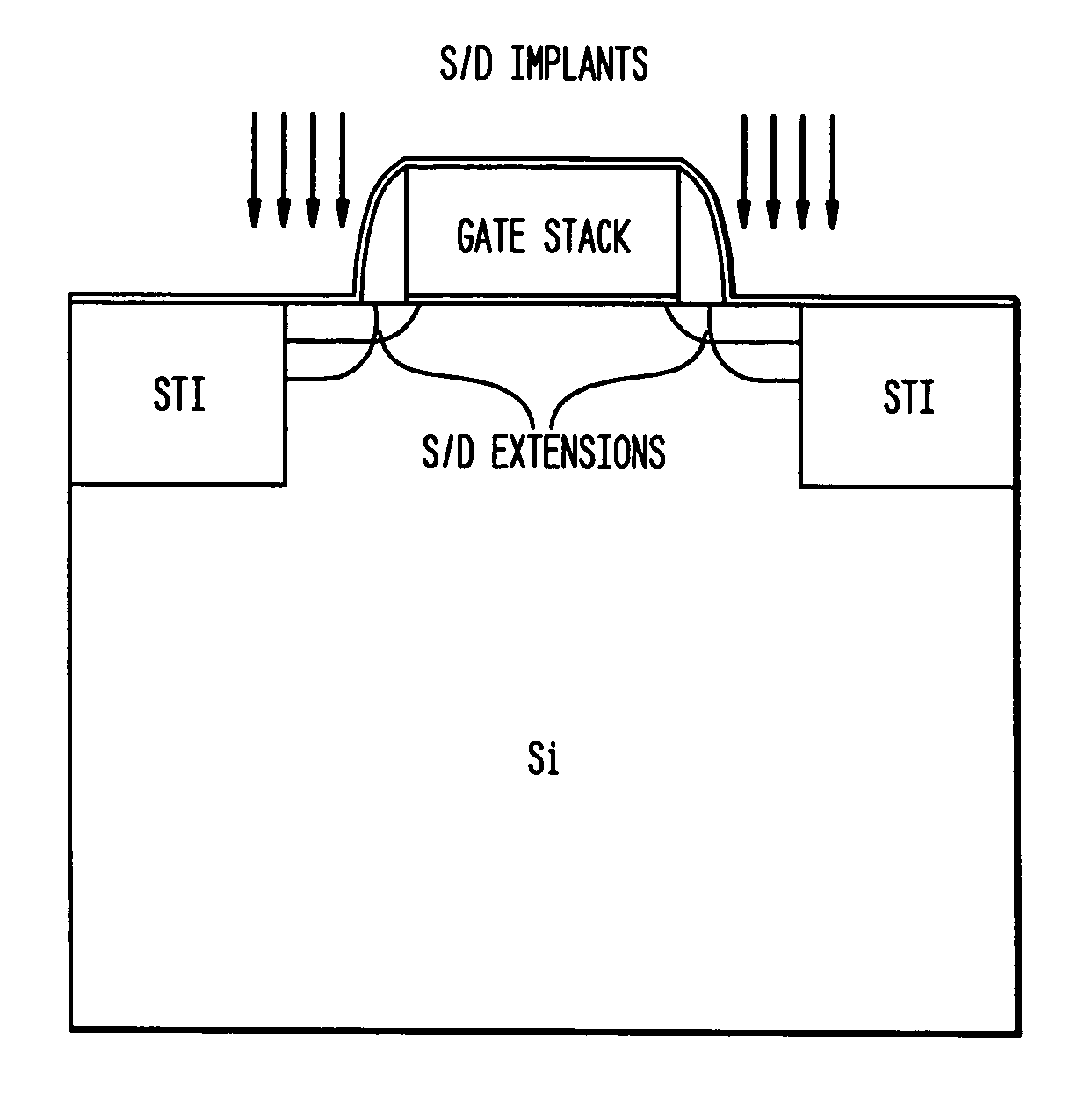
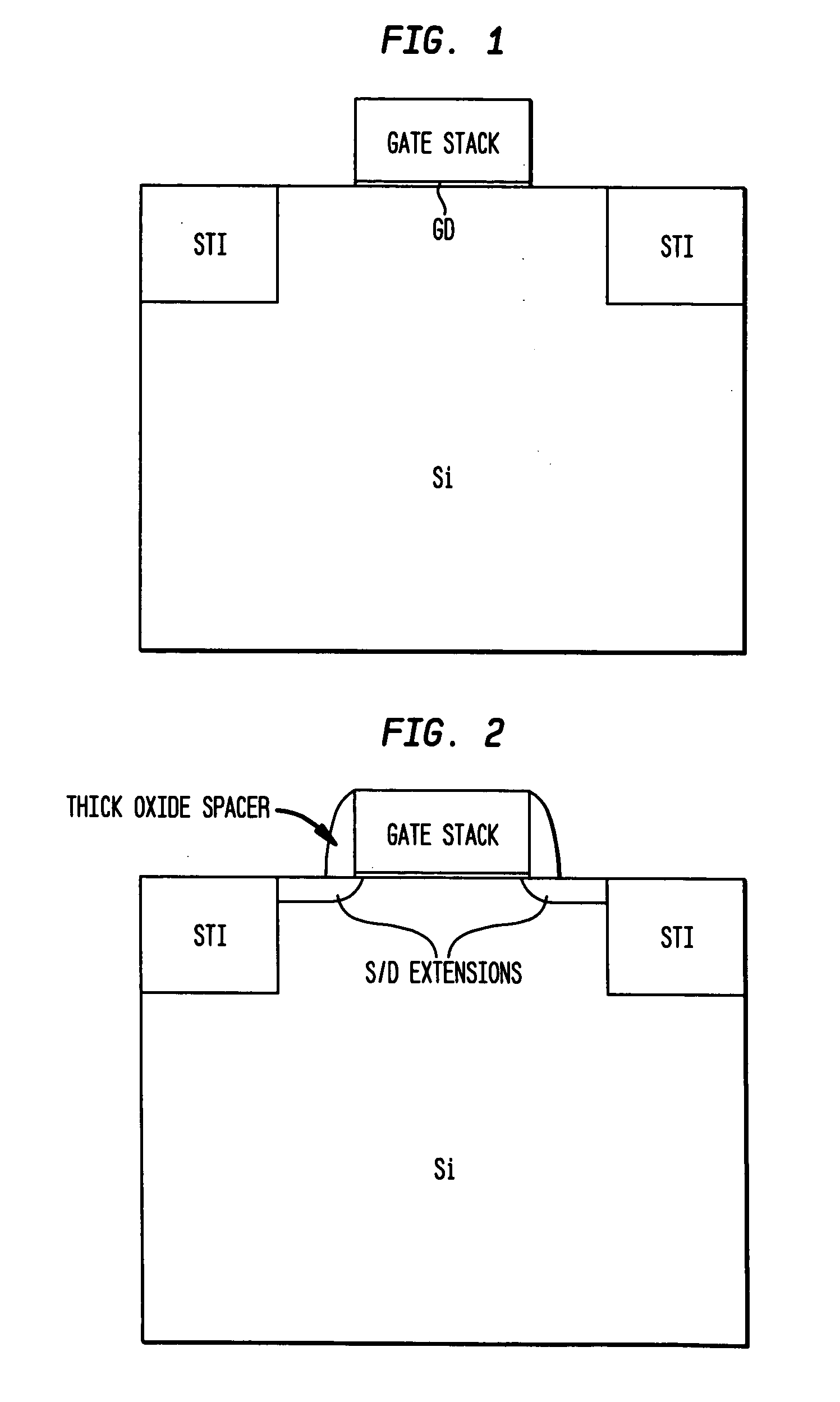
[0031]FIG. ...


PUM


Abstract

A MOSFET device and a method of fabricating a MOSFET device having low-K dielectric oxide gate sidewall spacers produced by fluorine implantation. The present invention implants fluorine into the gate oxide sidewall spacers which is used to alter the properties of advanced composite gate dielectrics e.g. nitridized oxides, NO, and gate sidewall dielectrics, such that the low-K properties of fluorine are used to develop low parasitic capacitance MOSFETs.

Description

CROSS REFERENCE TO RELATED APPLICATION[0001]The present application is a divisional of U.S. patent application Ser. No. 10 / 345,344, filed on Jan. 15, 2003 now U.S. Pat. No. 6,720,213.BACKGROUND OF THE INVENTION[0002]The present invention relates generally to the provision of low-K (reduced from 4.0 to approximately 3.3) gate sidewall spacers by fluorine implantation in a MOSFET device, and more particularly pertains to a MOSFET structure, and a method of fabrication thereof, having fluorine doped gate oxide sidewall spacers, such that the low-K properties of fluorine are used to develop low parasitic capacitance MOSFETs[0003]Device feature scaling has associated fundamental problems which tend to degrade overall power dissipation including:[0004]increased stud or via capacitance as a result of sidewall spacer thickness reduction;[0005]increased overlap capacitance as a result of gate dielectric thickness scaling;[0006]increased GIDL (gate-induced drain leakage) current as a result o...

Claims


Application Information

Patent Timeline
IPC IPC(8): H01L29/76H01L29/94H01L31/062H01L31/113H01L31/119H01L21/265H01L21/3115H01L21/336H01L29/49
CPCH01L21/31155H01L29/4983H01L29/6659H01L21/26506H01L21/26586H01L29/6656Y10S257/90
Inventor GAMBINO, JEFFREY P.MANDELMAN, JACKTONTI, WILLIAM R.
Owner GLOBALFOUNDRIES US INC
Why Eureka
Try Eureka