High density plasma oxidation

a plasma oxidation and high density technology, applied in the field of high density plasma oxidation, can solve the problems of high undesirable single-wallet oxidation process longer than 5 minutes, inability to quickly recombine, and inability to provide a uniform distribution of atomic oxygen over a relatively large substrate (200-mm in diameter and larger) , to achieve the effect of high oxide uniformity

a plasma oxidation and high density technology, applied in the field of high density plasma oxidation, can solve the problems of high undesirable single-wallet oxidation process longer than 5 minutes, inability to quickly recombine, and inability to provide a uniform distribution of atomic oxygen over a relatively large substrate (200-mm in diameter and larger) , to achieve the effect of high oxide uniformity

US7273638B2Inactive Publication Date: 2007-09-25INT BUSINESS MASCH CORP +1

Image

  • High density plasma oxidation
  • High density plasma oxidation
  • High density plasma oxidation

Examples


Embodiment Construction

)

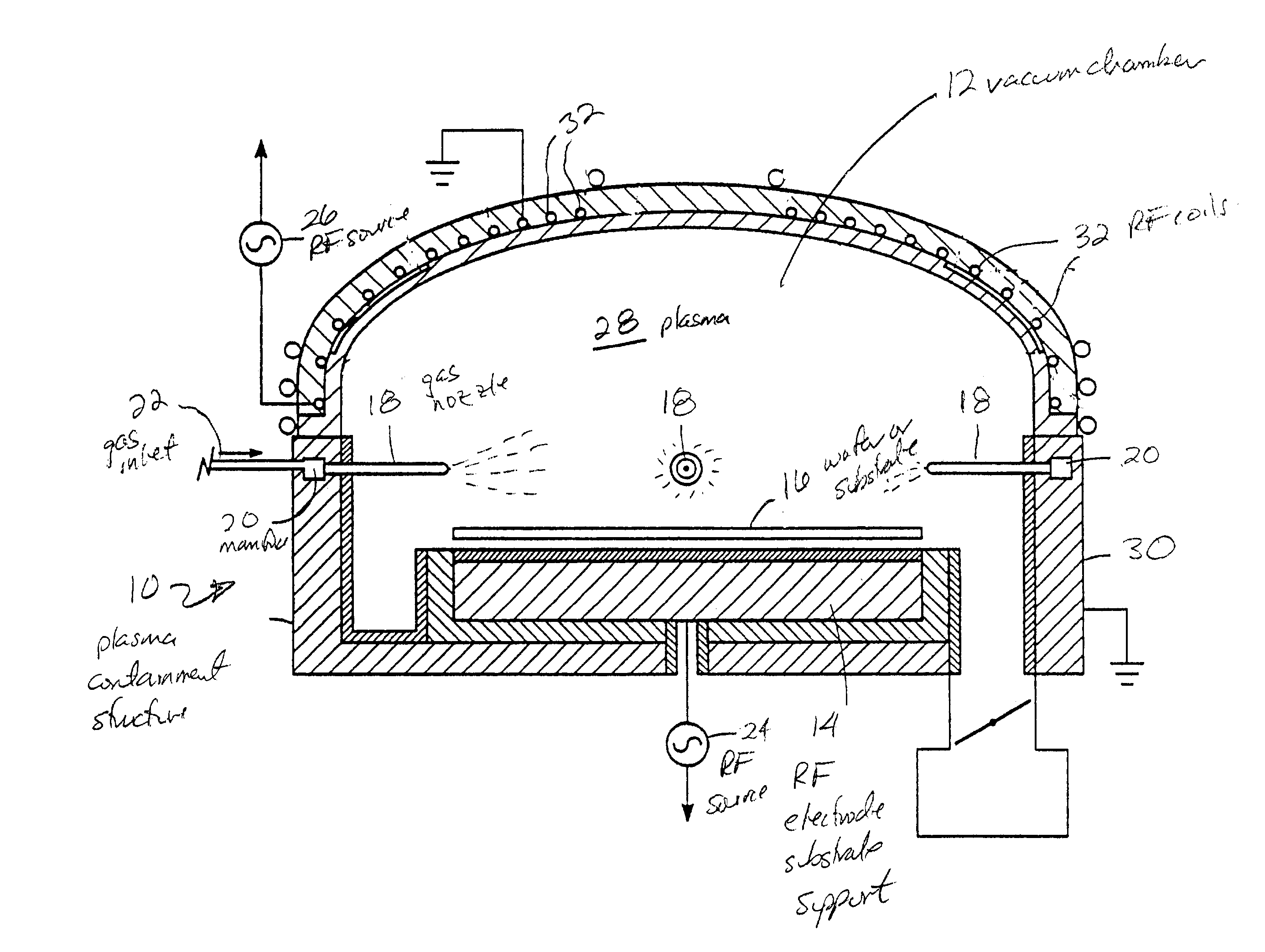
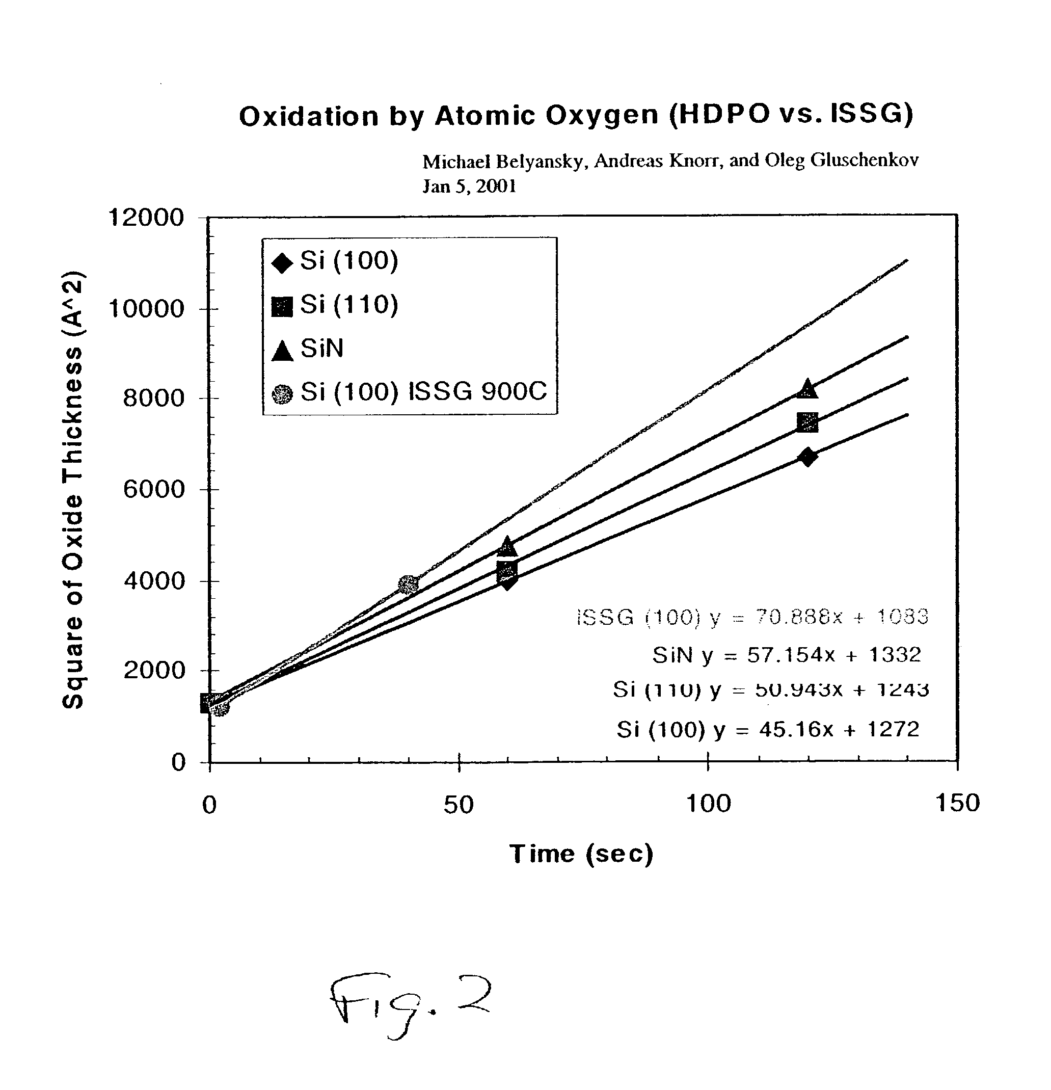
[0025]In describing the preferred embodiment of the present invention, reference will be made herein to FIGS. 1 and 2 of the drawings in which like numerals refer to like features of the invention. Features of the invention are not necessarily shown to scale in the drawings.

[0026]The present invention provides a method and system for oxidizing semiconductor substrates which utilizes a readily commercially available high density plasma reactor of the type normally used for chemical vapor deposition (CVD). The substrate or wafer can be comprised of either conductors (e.g., elemental metals, metal suicides, certain metal nitrides, and the like), semiconductors (e.g., Si, Ge, SiGe, SiC, SiGeC, or any of III-V or II-VI compounds), insulators and insulating ceramics (e.g. glass, sapphire, silicon nitride, boron nitride, etc.), and polymers. The substrate can have multiple layers of these materials (e.g. silicon-on-insulator (SOI) and silicon-germanium-on-insulator (SGOI) substrates, stra...


PUM

PropertyMeasurementUnit
surface areaaaaaaaaaaa
electron densityaaaaaaaaaa
mole fractionaaaaaaaaaa

Abstract

A method of oxidizing a substrate having area of about 30,000 mm2 or more. The surface is preferably comprised of silicon-containing materials, such as silicon, silicon germanium, silicon carbide, silicon nitride, and metal suicides. A mixture of oxygen-bearing gas and diluent gas normally non-reactive to oxygen, such as Ne, Ar, Kr, Xe, and / or Rn are ionized to create a plasma having an electron density of at least about 1e12 cm−3 and containing ambient electrons having an average temperature greater than about 1 eV. The substrate surface is oxidized with energetic particles, comprising primarily atomic oxygen, created in the plasma to form an oxide film of substantially uniform thickness. The oxidation of the substrate takes place at a temperature below about 700° C., e.g., between about room temperature, 20° C., and about 500° C.

Description

BACKGROUND OF THE INVENTION[0001]1. Field of the Invention[0002]The present invention relates to a method and system for oxidizing surfaces and, in particular, is directed to oxidizing silicon-containing and other semiconductor wafers in a high-density plasma chemical vapor deposition tool.[0003]2. Description of Related Art[0004]In general, an oxidation process is performed by heating wafers in an ambient of oxygen-bearing gas. Typical oxygen-bearing gases are molecular oxygen O2, water vapors H2O, nitrous oxide N2O, nitric oxide NO, and ozone O3. Oxidation reactors can be roughly divided into single wafer tools and furnaces. A typical oxidation furnace processes many wafers at once. Modern oxidation furnaces can process 100-200 200-mm-diameter wafers in one batch. Due to the large batch size, the furnaces can support relatively slow processes without affecting throughput. A typical furnace throughput is 50-100 wafers per hour. On the other hand, single wafer tools process one wafe...

Claims


Application Information

Patent Timeline
25 Sep 2007
Publication
US7273638B2
IPC
H05H1/46; B05D3/06; B05D3/14; C23C16/40; C23C16/505; C23C16/509; H01L21/473; C23C8/36; H01L21/316
CPC
C23C8/36; H01J37/321; H01L21/02236; H01L21/02238; H01L21/02252; H01L21/31658; H01L21/31662; H01J2237/338
Inventors
BELYANSKY, MICHAEL; GLUSHENKOV, OLEG