Direct write process and apparatus

a technology of direct writing and process, which is applied in the direction of process and machine control, recording apparatus, instruments, etc., can solve the problems of insufficient application insufficient use of large-scale rapid prototyping techniques, and insufficient use of large-scale rapid prototyping methods, etc., to achieve rapid device prototyping and manufacturing, good combination of device accuracy and fabrication rate, and low-volume production run cost-effective

Active Publication Date: 2007-10-02
NANOTEK INSTR GRP LLC
View PDF7 Cites 51 Cited by
  • Summary
  • Abstract
  • Description
  • Claims
  • Application Information

AI Technical Summary

Benefits of technology

[0021]Alternatively, the constant but adjustable pressure may be achieved by using a compressed air source and an adjustable pressure-regulating valve. The purpose of varying the pressure imposed on the fluid material is to achieve a good control over the droplet size of the fluid material discharged out of the orifice and the volume flow rate. The volume flow rate governs the over-all device-fabricating speed. A smaller pressure, hence a smaller amount of liquid droplets ejected in a given time period, may be used to fabricate boundary or periphery areas of a component or any fine features where component dimensional accuracy is a requirement. Once the peripheries of a component or contour lines of a layer are built with good surface finish or component accuracy, the interior of a component or a layer could be quickly filled in by dispensing a larger volume of fluid material through the same orifice. This is readily accomplished in real time during the dispensing step by simply increasing the chamber pressure that drives the flow of the material. This capability makes it possible to achieve both component dimensional accuracy and fabrication rate, which are normally considered as mutually exclusive in conventional rapid prototyping or direct write technologies.
[0022]In step (d), the dispensed material may be heat- or energy-treated by a means selected from the group consisting of a ventilation fan, a vacuum pump, an air blower, a cooling device, a heater, an ultraviolet light source, an infrared source, a laser beam, an electron beam, an X-ray source, a Gamma-ray source, an ion beam source, a microwave source, an induction generator, and combinations thereof. The purpose of executing this procedure is to convert the deposited precursor material to the component of a desired composition and physical state (e.g., solid state). In the process used to fabricate a multiple-layer device, this heat treatment step brings the component materials of a layer just dispensed to a sufficiently rigid physical state so that this layer can support its own weight and the weight of subsequently deposited layers without incurring an excessive dimensional change.
[0026]Highly Versatile Process: The present invention provides a simple yet versatile process of rapid device prototyping and manufacturing. A user is free to choose the precursor fluid materials from a wide spectrum of material compositions. Further, two or three materials may be combined to form a mixture, a composite, or a reaction product that constitutes a component with a desired combination of physical, chemical and electronic properties. There is essentially no constraint imposed on the kind of materials that can be fabricated into passive or active components of a microelectronic device.
[0027]Rapid Device Prototype Fabrication for Functional Testing: A prototype device may be designed and made to be similar or identical in both component compositions and geometric arrangement to the production device. Hence, the device prototype can be fully evaluated to verify the functional performance of a device before a photo-lithographic mask is fabricated (which is extremely expensive) or before mass production begins. This could help eliminate the possibility of producing an un-suitable mask or a large number of devices only to find out that these devices do not meet the functional requirements.
[0028]Cost-Effective Low-Volume Production Runs and Rapid Device Manufacturing: Rapid manufacturing of devices can be achieved in a more cost-effective fashion by using the presently invented process and apparatus, particularly when only a small number of identical devices (e.g., from 1 to 1,000) at a given time. With a higher back pressure, inkjet printing becomes possible essentially for most of the materials used in active or passive components commonly found in a micro-electronic device. A higher and stable back pressure leads to a much higher fluid dispensing rate. We have surprisingly found that a material deposition rate at a line speed of several meters per second is achievable with the present process and apparatus. This feature makes the present technology amenable to mass production of microelectronic devices, not just low-volume production runs.
[0029]Simple and Less Expensive Fabrication Equipment: Polymer melts or solution are normally highly viscous and, hence, difficult to eject out of a small orifice due to a high capillarity pressure that must be overcome. A suspension with a high solid content is also highly viscous (does not flow well). The presently invented fluid material delivery assembly and printhead system now makes it possible to dispense highly viscous fluids in ultra-fine droplets. The equipment is simple, reliable, and inexpensive. For instance, one can now easily convert a 2-D inkjet printer commonly used in an office environment to become a direct-write fabricator of micro-electronic devices. Sheets of paper may simply be replaced by sheets of plastic substrate, for instance, for flexible electronic device fabrication. Commercially available 2-D inkjet printers are normally rated at an operable ink viscosity of up to 10–20 cps only. By incorporating a presently invented variable back pressure device to the ink container in a black or color ink cartridge, and by replacing the black or color inks by a precursor fluid (e.g., using a syringe needle), a 2-D inkjet printer can now print out essentially all the conceivable precursor fluid materials for micro-electronic device fabrication.

Problems solved by technology

Although DWM may also be accomplished in the sub-micron range using electron beams or focused ion beams, these techniques are not appropriate for large scale rapid prototyping due to their small scale and, hence, low deposition rates.
Due to the film material being vaporized by the action of the laser, LIFT is inherently a homogeneous, pyrolytic technique and typically cannot be used to deposit complex crystalline or multi-component materials.
Furthermore, because the material to be transferred is vaporized, it becomes more reactive and can more easily become degraded, oxidized or contaminated.
The method is not well suited for the transfer of organic materials, since many organic materials are fragile and thermally labile and can be irreversibly damaged during deposition.
Other shortcomings of the LIFT technique include poor uniformity, morphology, adhesion, and resolution.
Further, because of the high temperatures involved in the process, there is a danger of ablation or sputtering of the support, which can cause the incorporation of impurities in the material being deposited on the receiving substrate.
For some intended transfer materials, it may be difficult to find a suitable matrix material that is physically and chemically compatible with the transfer material so that the “lifting” procedure can be properly carried out.
Since a pulsed laser is also used in the MAPLE technique, this technique suffers from similar drawbacks that are commonly associated with the LIFT process.
Heavy and expensive equipment is required in these processes.
Due to the limited allowable liquid viscosity range (typically up to 20 centi-poise, cps, only) of a printhead, 3-D inkjet printing has been limited to wax and other low-molecular weight polymers.
These conventional print-heads for 2-D color printing or 3-D object printing are not directly amenable to the deposition of passive or active electronic components or elements onto a silicon or plastic substrate.
These precursor fluids, when with a low solid content (or with a low proportion of the precursor material being actually converted into the final component), may be directly injectable by a conventional inkjet print-head, but resulting in extremely thin film deposited on a solid substrate.
On the other hand, a precursor fluid containing a higher solid or desired component content normally has too high a fluid viscosity (easily greater than 20 cps) to be directly injectable by a conventional inkjet print-head.
In addition to the above-cited problem of being incapable of dispensing higher-viscosity or higher solid content fluid, the conventional inkjet printing devices suffer from the following shortcomings: (1) limited range of materials that can be inkjet printed and, hence, limited scope of application in direct writing of microelectronic components; and (2) difficulty or incapability in adjusting the fluid dispensing rate on demand or in real time during the component fabrication procedure.

Method used


Image

  • Direct write process and apparatus
  • Direct write process and apparatus
  • Direct write process and apparatus

Examples


Embodiment Construction

Process and Apparatus:

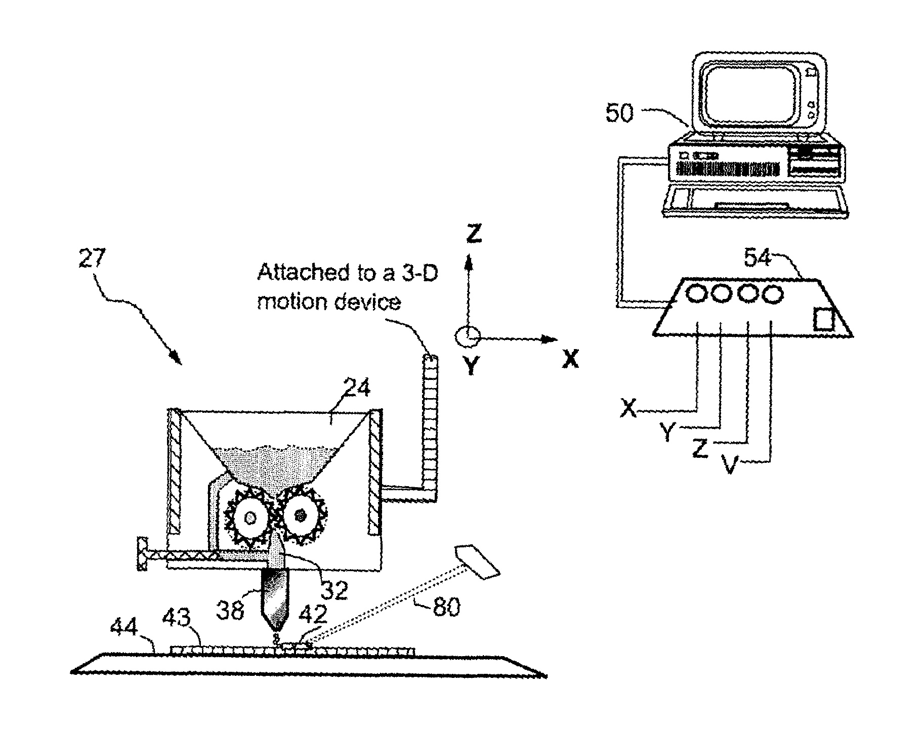
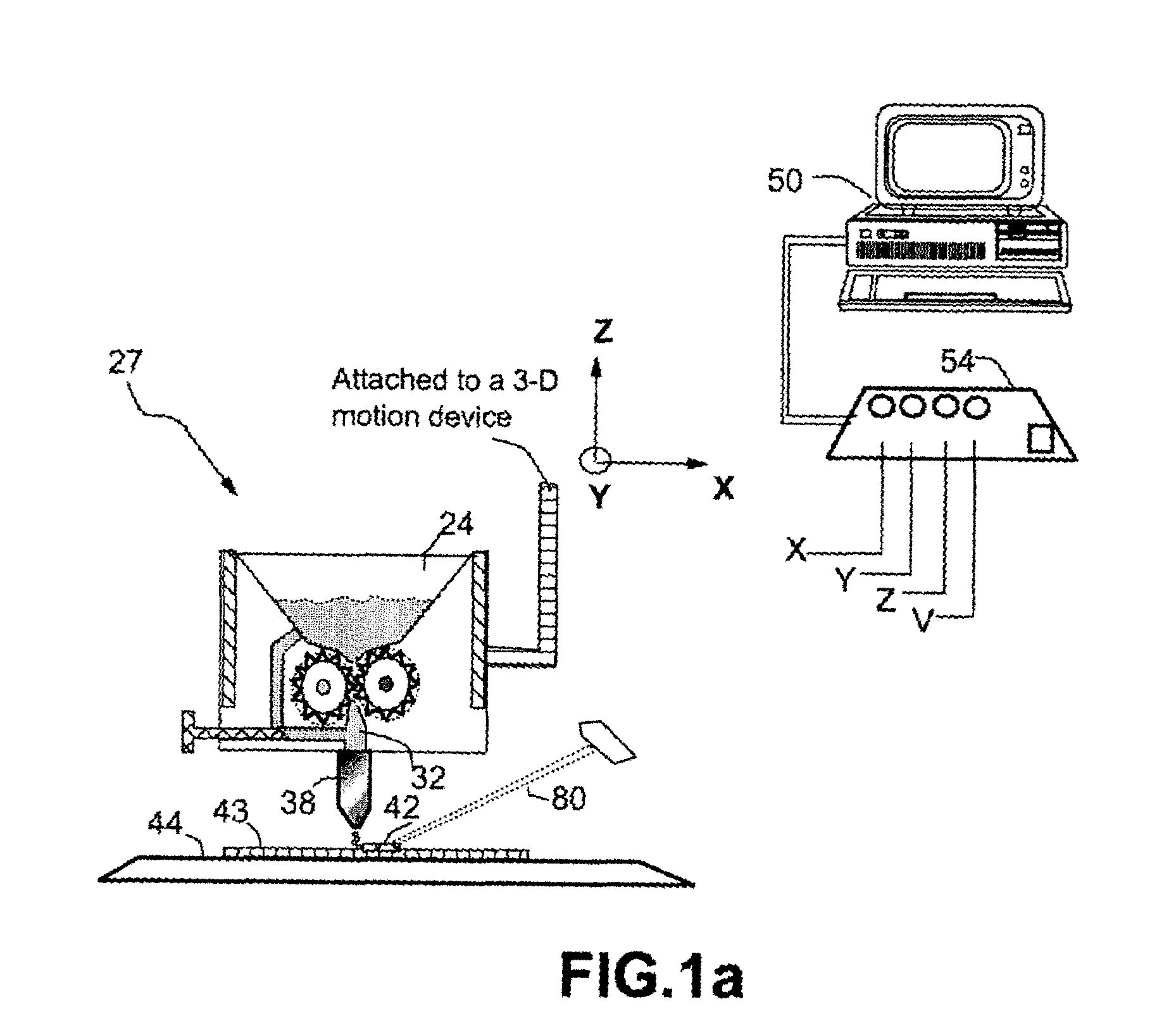
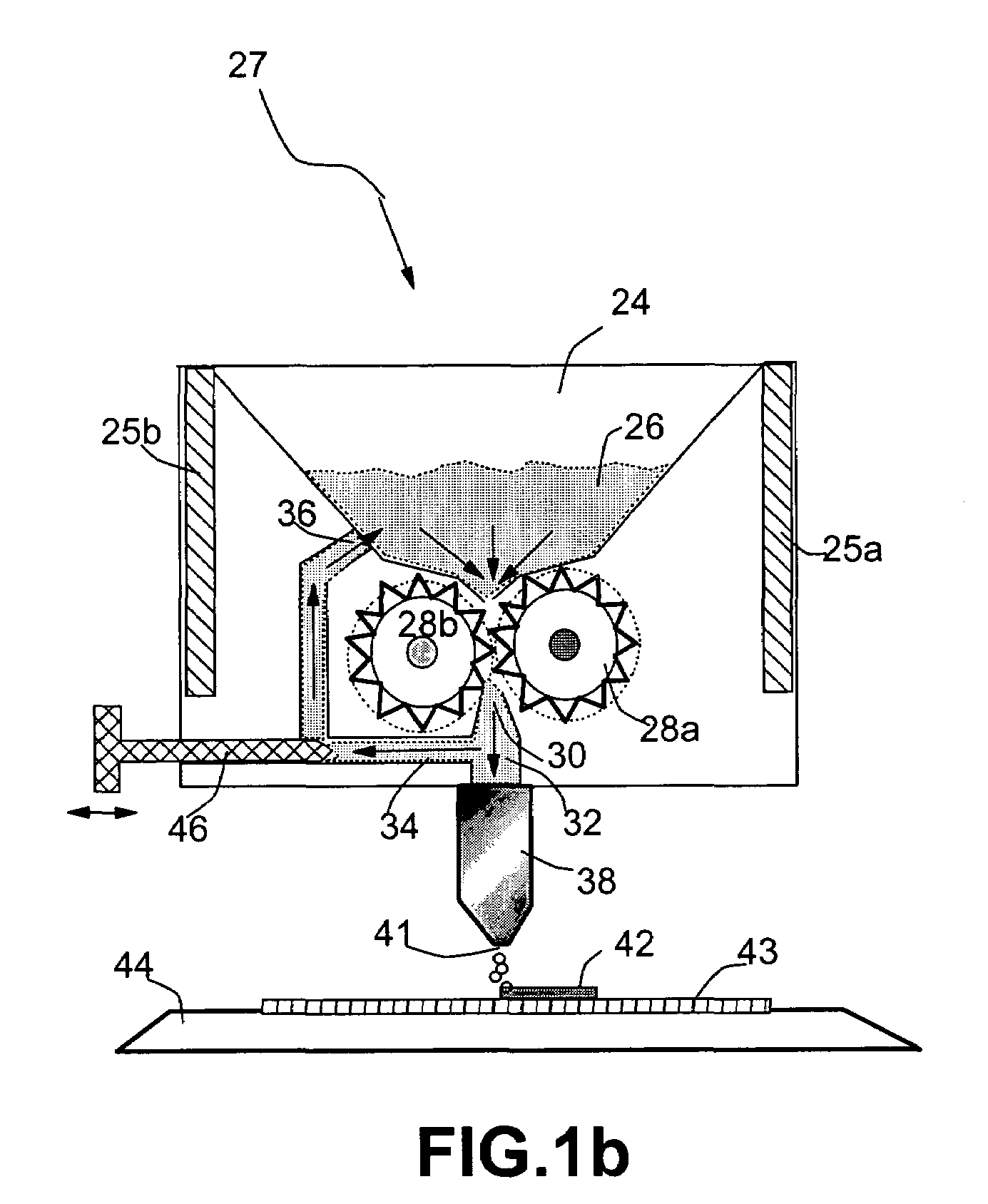
[0037]FIG. 1(a) illustrates one preferred embodiment of the presently invented process and apparatus for fabricating passive or active components onto a substrate surface to make a micro-electronic device, preferably on a point-by-point basis. The process begins with the creation of a computer-aided design (CAD in the form of a drawing, image, or geometry representation) of the device using a computer 50. This method further involves the operation of a system that includes computer software and control hardware, e.g., motion controller / indexer / servo 54. The system includes a support member 44 by which the device substrate 43 is supported while the device components are being deposited. The system also has an inkjet printhead-based dispensing head 38 for dispensing liquid droplets from a precursor fluid material 26. This material includes a liquid ingredient that helps to make the material in a flowable state while still residing in a chamber 32 of the dispensin...


PUM

PropertyMeasurementUnit
viscosityaaaaaaaaaa
operating temperatureaaaaaaaaaa
pressureaaaaaaaaaa

Abstract

A direct write process and apparatus for fabricating a desired circuit component onto a substrate surface of a microelectronic device according to a computer-aided design (CAD). The process includes (a) providing a support member by which the device is supported while being fabricated; (b) providing a chamber for containing a precursor fluid material under a substantially constant pressure differential relative to the ambient pressure, with the precursor fluid material having a viscosity no less than 10 cps; (c) operating an inkjet-based dispensing head with a control valve or actuator for dispensing and depositing minute droplets of the precursor fluid material onto the substrate surface; (d) energy- or heat-treat the deposited precursor fluid material for converting it to the desired active or passive component; and (e) operating a machine controller for generating control signals in response to the CAD coordinates for controlling the position of the dispensing head relative to the support member in response to the control signals to control dispensing and depositing of the precursor material to form the desired component. The process is useful for depositing a wide range of component materials onto an electronic device, including conductor, resistor, capacitor, dielectric, inductor, antenna, solar cell electrode, battery electrode, interconnect, superconductor, sensor, and actuator element materials.

Description

FIELD OF THE INVENTION[0001]This invention relates generally to a computer-controlled device-fabricating process and apparatus and, in particular, to an improved inkjet printing-based direct-write manufacturing process and apparatus for depositing desired active, passive, and other functional components to make an integrated circuit (IC) or a micro-electronic device such as a sensor, actuator, or micro-electro-mechanical system (MEMS).BACKGROUND OF THE INVENTION[0002]Direct write manufacturing (DWM) involves creating a pattern of active, passive and other functional components or elements directly onto a solid substrate, either by adding or removing material from the substrate, without utilizing a mask, pre-existing form, or tooling. DWM technologies were developed to answer the need of the microelectronics industry to have a means for rapidly prototyping circuit elements on various substrates. These elements are typically at the mesoscopic scale, i.e., within a size range between c...

Claims


Application Information

Patent Timeline
Patent Type & Authority Patents(United States)
IPC IPC(8): G06F19/00B05D5/00G05D7/00B29C41/02B29C41/20B29C67/00
CPCB29C41/02B29C67/0059B29C41/20B29C64/112B33Y30/00B33Y10/00B33Y50/02
Inventor HUANG, WEN C.
Owner NANOTEK INSTR GRP LLC
Why Eureka
Try Eureka