
Method for manufacturing contact structures of wirings

Inactive Publication Date: 2007-10-30
SAMSUNG DISPLAY CO LTD
View PDF17 Cites 2 Cited by
  • Summary
  • Abstract
  • Description
  • Claims
  • Application Information

AI Technical Summary

Benefits of technology

[0008]It is therefore an object of the present invention to provide contact structures having good contact properties of wiring made of a material of low resistivity and methods for manufacturing the same.
[0010]It is another object of the present invention to simplify manufacturing methods of thin film transistor array panels for liquid crystal displays.

Problems solved by technology

However, the physical and the chemical properties of the aluminum or aluminum alloy is not good.
In other words, the aluminum or aluminum alloy is easily oxidized and broken, when connecting other conductive material in a contact portions.
Accordingly, the characteristics of semiconductor devices are deteriorated.
Especially, it causes problems when ITO (indium tin oxide) as a transparent electrode such as in a liquid crystal display is used to reinforce pad portions of aluminum.
However, because of the poor contact properties between aluminum or aluminum alloy and indium tin oxide (ITO), the aluminum or aluminum alloy must be removed to prevent the corrosion of aluminum and aluminum alloy and a different material is then inserted therebetween.
Accordingly, the manufacturing method is complicated and production costs are increased.
Since the photolithography process is expensive, the number of the photolithography steps needs to be minimized.

Method used


Image

  • Method for manufacturing contact structures of wirings
  • Method for manufacturing contact structures of wirings
  • Method for manufacturing contact structures of wirings

Examples


first embodiment

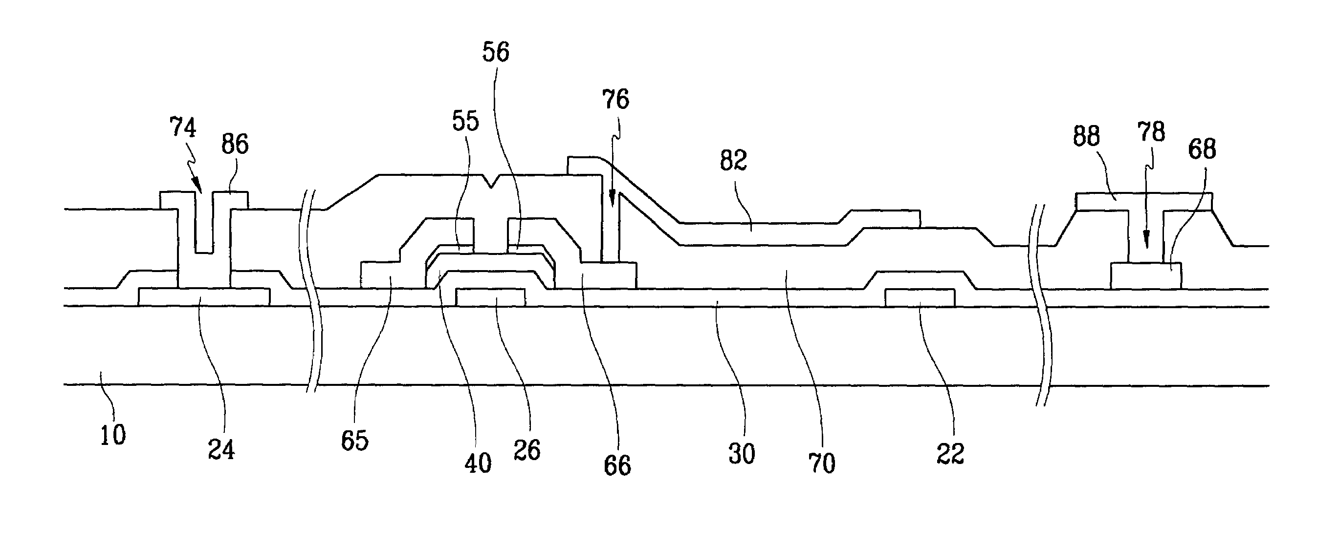
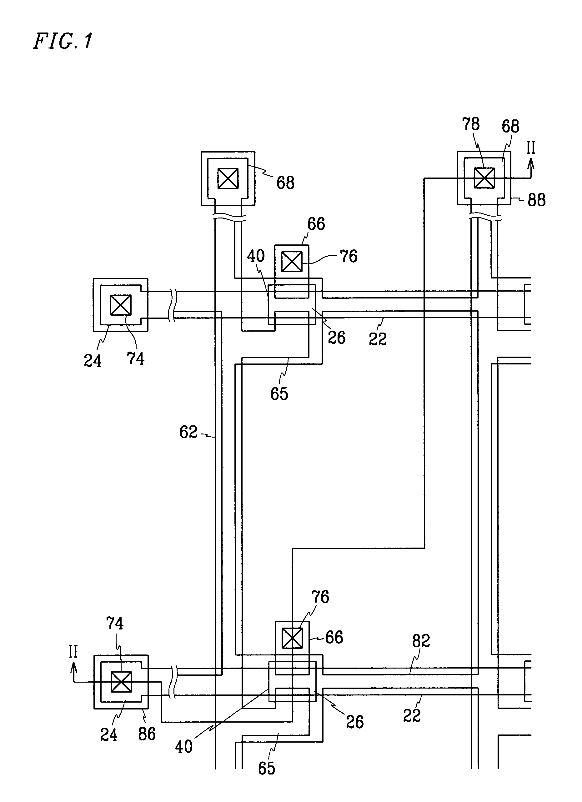
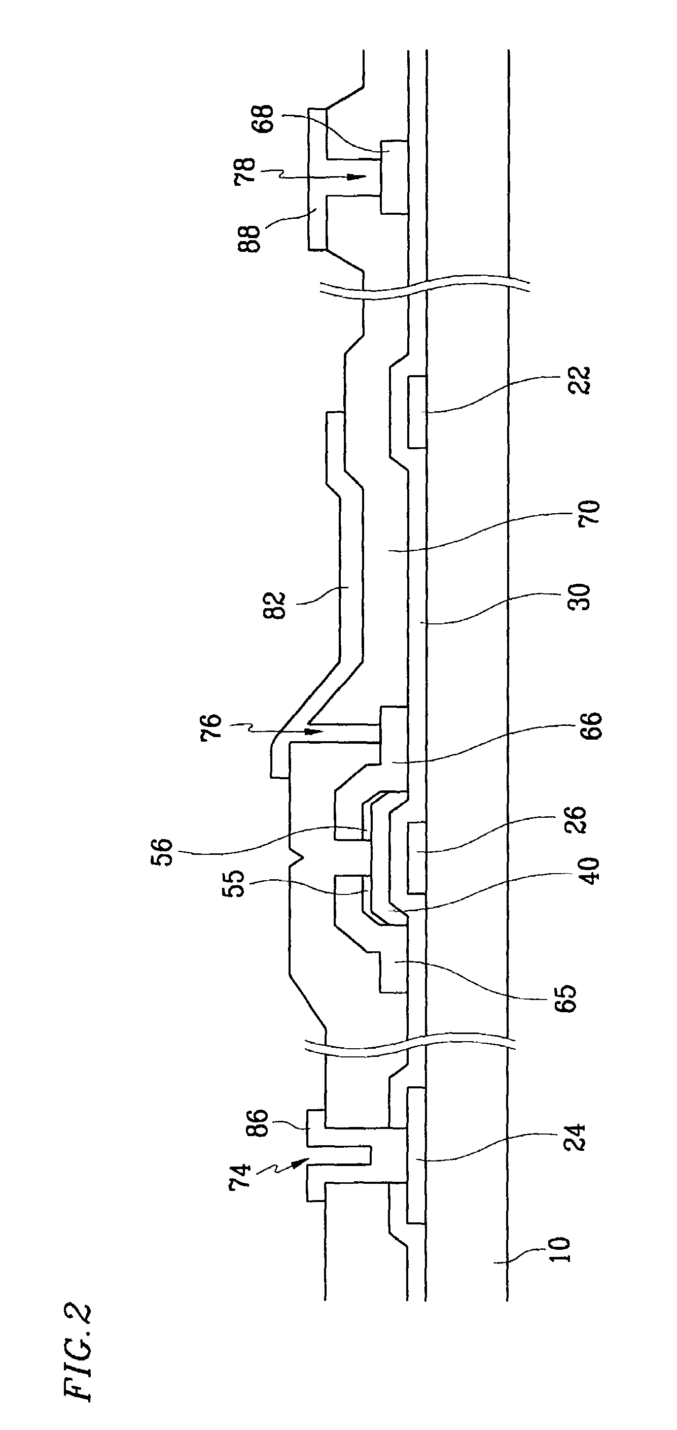
[0049]First, the structure of a TFT array panel for a liquid crystal display according to present invention will now be described specifically with reference to FIGS. 1 and 2.

[0050]FIG. 1 is a layout view of a thin film transistor array panel for a liquid crystal display according to the first embodiment of the present invention, and FIG. 2 is a cross-sectional view taken along line II-II′ of FIG. 1.

[0051]Gate wires made of conductive material having a low resistivity, such as aluminum (Al) or aluminum alloy (Al alloy), is formed on an insulating substrate 10. A gate wire includes a gate line (or scanning signal line) 22 extending in the horizontal direction in FIG. 1, a gate pad 24 connected to an end of the gate line 22 and which transmits a scanning signal from an external circuit to the gate line 22, and a gate electrode 26 which is a part of a thin film transistor and connected to the gate line 22.

[0052]A gate insulating layer 30 of silicon-nitride (SiNx) is formed on and cover...

second embodiment

[0072]FIG. 7 is a layout view of a thin film transistor array panel for a liquid crystal display according to the present invention, and FIGS. 8 and 9 are the cross-sectional views taken along lines XIII-XIII′ and IX-IX′ of FIG. 7.

[0073]Gate wires made of metal or conductive material such as aluminum (Al) or aluminum alloy and including a gate line 22, a gate pad 24 and a gate electrode 26, like the first embodiment, are formed on an insulating substrate 10. Also, the gate wires includes a storage electrode 28 that is formed parallel with the gate line 22 and receives a voltage such as a common voltage applied to a common electrode (not shown) on an upper panel of the liquid crystal display. The storage electrode 28 provides storage capacitance along with a conductor pattern 68 connected to a pixel electrode 82 that will be described later. The liquid crystal capacitor includes the pixel electrode 82 and the common electrode. The storage electrode 28 may not be provided if the stora...


PUM


Abstract

First, a conductive material of aluminum-based material is deposited and patterned to form a gate wire including a gate line, a gate pad, and a gate electrode. A gate insulating layer is formed by depositing nitride silicon in the range of more than 300° C. for 5 minutes, and a semiconductor layer and an ohmic contact layer are sequentially formed. Next, a conductor layer of a metal such as Cr is deposited and patterned to form a data wire include a data line intersecting the gate line, a source electrode, a drain electrode and a data pad. Then, a passivation layer is deposited and patterned to form contact holes exposing the drain electrode, the gate pad and the data pad. Next, indium zinc oxide is deposited and patterned to form a pixel electrode, a redundant gate pad and a redundant data pad respectively connected to the drain electrode, the gate pad and the data pad.

Description

CROSS REFERENCE[0001]This is a divisional application of the U.S. patent application Ser. No. 09 / 837,374 filed on Apr. 19, 2001 now U.S. Pat. No. 6,630,688.BACKGROUND OF THE INVENTION[0002](a) Field of the Invention[0003]The present invention relates to contact structures of wirings and methods for manufacturing the same, and thin film transistor array panels including the same and methods for manufacturing the same.[0004](b) Description of the Related Art[0005]Generally, wiring of semiconductor devices is to transmit signals without delay.[0006]In order to prevent delay or distortion of signals, materials having a low resistivity such as aluminum or aluminum alloys are generally used. However, the physical and the chemical properties of the aluminum or aluminum alloy is not good. In other words, the aluminum or aluminum alloy is easily oxidized and broken, when connecting other conductive material in a contact portions. Accordingly, the characteristics of semiconductor devices are ...

Claims


Application Information

Patent Timeline
IPC IPC(8): H01L21/84H01L21/00G02F1/1333G02F1/1368H01L21/28H01L21/3205H01L21/336H01L21/768H01L21/77H01L23/52H01L23/532H01L27/12H01L29/45H01L29/786
CPCG02F1/13439G02F1/13458H01L21/76801H01L21/76838H01L23/53209H01L27/124H01L29/458H01L27/1288H01L27/12H01L2924/0002H01L2924/00G02F1/136
Inventor KONG, HYANG-SHIKHUR, MYUNG-KOOKIM, CHI-WOO
Owner SAMSUNG DISPLAY CO LTD
Learn More