Semiconductor manufacturing method

Inactive Publication Date: 2007-12-11
SEMICON ENERGY LAB CO LTD
View PDF54 Cites 49 Cited by
  • Summary
  • Abstract
  • Description
  • Claims
  • Application Information

AI Technical Summary

Benefits of technology

[0080]Since the energy given by the laser of continuous oscillation is large, it is possible to crystallize the double-layered semiconductor layer by one laser irradiation processing. If necessary, the laser irradiation processing may be repeated several times. Also, although the laser beam incident the substrate is reflected at the surface of the substrate, since the laser beam is light having a high directivity and energy density, a damper may be provided to absorb the reflected light in order to prevent the reflected light from irradiating undesired area. According to the invention, it is possible to absorb the reflected light at the surface of the substrate by the double-layered semiconductor, since almost every laser beam can be absorbed by providing a double-layered or more semiconductor layer, particular damper may not be provided. Furthermore, since it is also possible to absorb the reflected light of the semiconductor layer of the lower layer by carrying out the irradiation again to the semiconductor layer of the upper layer, it is possible to irradiate the laser beam to the semiconductor layer effectively. Further, by repeating the reflection b

Problems solved by technology

In the case that the elements are disposed on a plane, since the required area allowed to occupy is limited, when the area is limited, a limitation resides therein.
Also, in a design that the elements are piled up, for e

Method used


Image

  • Semiconductor manufacturing method
  • Semiconductor manufacturing method
  • Semiconductor manufacturing method

Examples


embodiment 1

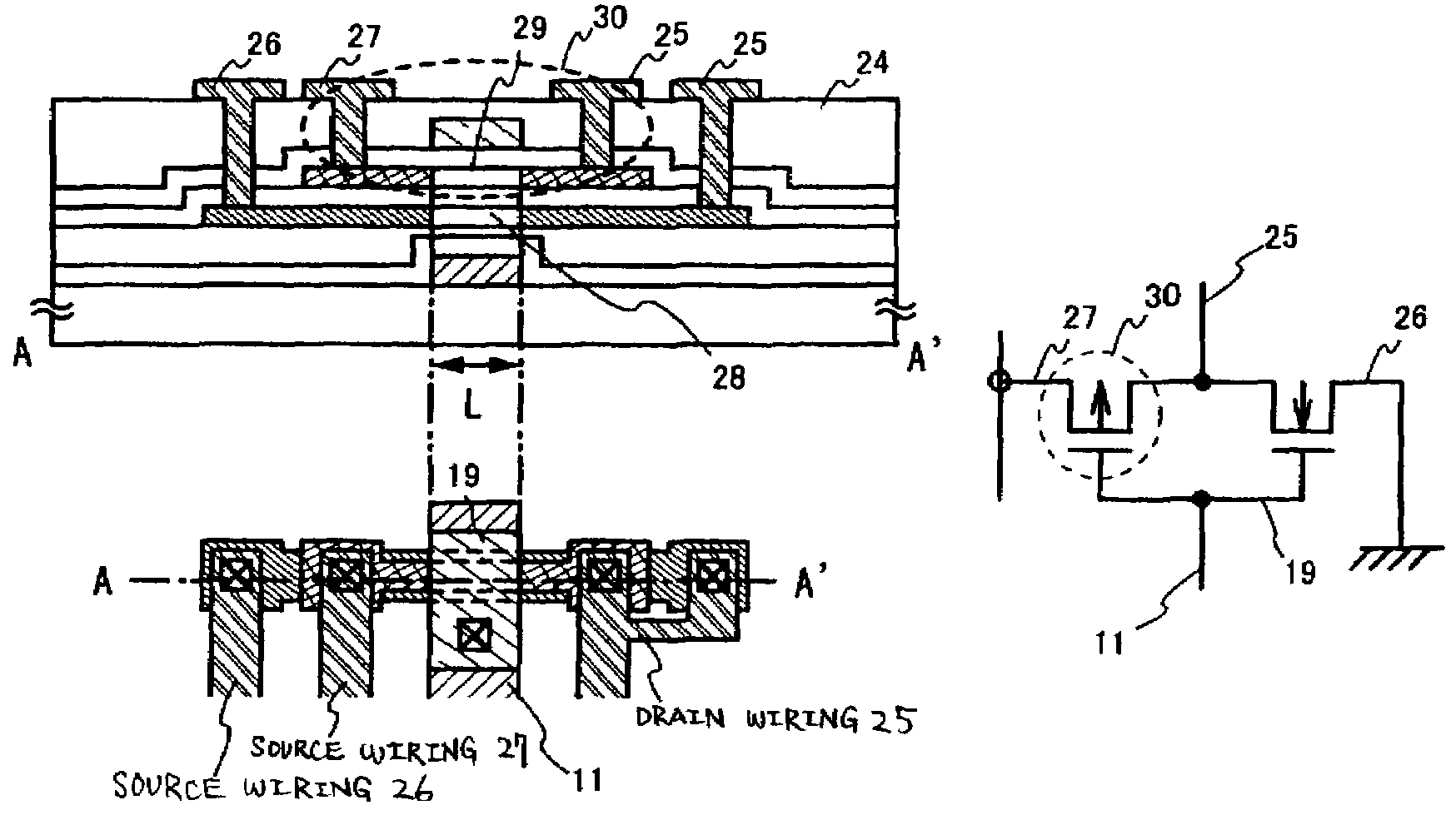
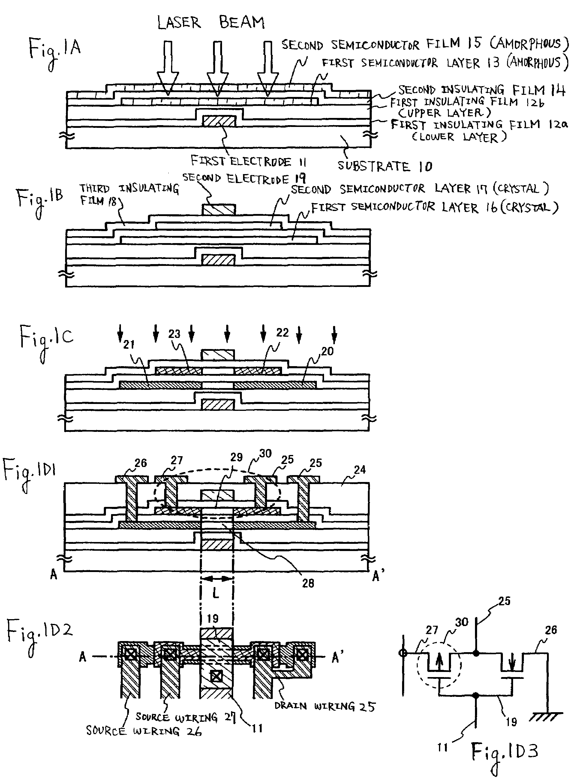
[0137]FIG. 1 briefly show a typical semiconductor device to which the invention is applied and a manufacturing method thereof. In this case, a description will be made while taking an inverter circuit as an example of CMOS circuit.

[0138]In FIG. 1A, reference numeral 10 denotes a substrate having insulated surface; reference numeral 11 denotes a first electrode; reference numerals 12a, 12b denote first insulating films; reference numeral 13 denotes a first semiconductor layer; reference numeral 14 denotes a second insulating film; and reference numeral 15 denotes a second semiconductor film.

[0139]In FIG. 1A, as for the substrate 10, a glass substrate, a quartz substrate, a ceramic substrate or a plastic substrate is applicable. As for the plastic substrate, since the heat resistance thereof is low, it is necessary to set the heat-treating temperature to a relatively low level, for example, to a temperature lower than 300° C.

[0140]First of all, as shown in FIG. 1A, the first electrode...

embodiment 2

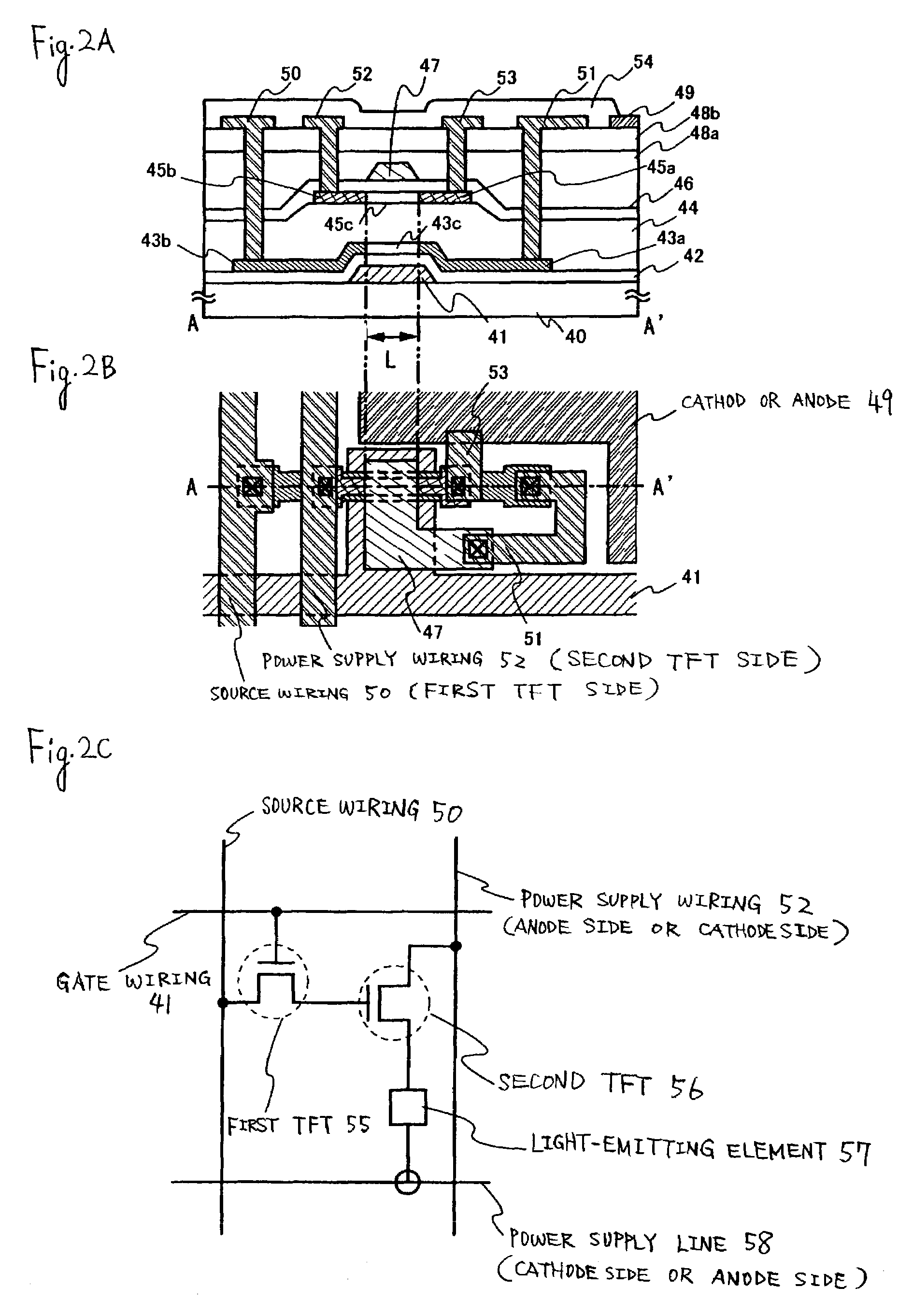
[0176]Hereinafter, referring to FIG. 2 and FIG. 3, a light-emitting device having a typical OLED, in which the invention is applied to, will be described. In this case, a light-emitting device, in which one pixel has two TFTs (first TFT 55, second TFT 56), will be described as an example.

[0177]In the sectional view shown in FIG. 2A, reference numeral 40 denotes a substrate; 41 denotes a first electrode (gate wiring); 42 denotes a first insulating film, 43a and 43b denote a source area or drain area, respectively; 43C denotes a channel forming area; 44 denotes a second insulating film; 45a denotes a source area; 45b denotes a drain area; 45c denotes a channel forming area; 46 denotes a third insulating film; 47 denotes a second electrode; 48a and 48b denote a fourth insulating film respectively; 49 denotes a cathode or anode; 50 denotes a source wiring; 51 denotes a connection electrode, 52 denotes a power supply wiring; 53 denotes a connecting electrode; and 54 denotes a bank.

[0178]...

embodiment 3

[0211]Hereinafter, a typical TFT, to which the invention is applied, and the manufacturing method thereof will be shown in FIG. 4; and FIG. 5 shows an example of a liquid crystal display device to which the invention is applied. In the Embodiments 1 and 2, examples, in which a plurality of TFTs having different constitution is formed respectively, were shown; in the Embodiment 3, a TFT having a plurality of channel forming areas will be described as an example.

[0212]First of all, on a substrate 70 having an insulated surface, a first insulating film 72, which will become a base insulating film, is formed. As for the first insulating film 72, a single or double layered insulating film comprised of silicon as the major component is formed. Although not shown in the figures, in this case, the first insulating film 72 is formed into a double-layered constitution. As the lower layer of the first insulating film 72, a silicon nitride / oxide film (composition ratio: Si=32%, O=27%, N=24%, H=...


PUM


Abstract

It is an object of the invention that, in semiconductor device, in order to promote the tendency of miniaturization of each display pixel pitch, which will be resulted in with the tendency toward the higher precision (increase of pixel number) and further miniaturizations, a plurality of elements is formed within a limited area and the area occupied by the elements is compacted so as to be integrated. A plurality of semiconductor layers 13, 15 is formed on different layers with insulating film 14 sandwiched therebetween. After carrying out crystallization by means of laser beam, on each semiconductor layer (semiconductor layers 16, 17 having crystal structure respectively), an N-channel type TFT of inversed stagger structure and a P-channel type TFT 30 of top gate structure are formed respectively and integrated so that the size of CMOS circuit is miniaturized.

Description

BACKGROUND OF THE INVENTION[0001]The present invention relates to a semiconductor device having a circuit constituted of a thin film transistor (hereinafter, referred to as TFT) and manufacturing method thereof. More particularly, the invention relates, for example, to an electrooptical device exemplified by a liquid crystal display panel and a light-emitting device exemplified by an electroluminescence display device and electronic apparatus on which electrooptical devices as described-above are mounted as component parts thereof.[0002]In this specification, the term “semiconductor device” means every device that functions by using the semiconductor characteristics; i.e., electrooptical devices, light-emitting devices, semiconductor circuits and electronic apparatuses are all included in the semiconductor device.[0003]Recently, a technique, in which a thin film transistor (TFT) is constituted using a semiconductor thin film (approximately several nm-several hundreds nm in thickness...

Claims


Application Information

Patent Timeline
IPC IPC(8): H01L21/84G02F1/1368G09F9/00G09F9/30G09F9/35H01L21/20H01L21/336H01L21/77H01L21/8238H01L27/00H01L27/092H01L27/12H01L27/32H01L29/786H01S3/00
CPCH01L27/1214H01L29/78648H01L29/66757H01L29/66765H01L29/78621G09G3/3208G09G2300/0857H01L27/3244H01L27/1251H01L27/127H01L27/1233H10K59/12
Inventor KUWABARA, HIDEAKITANAKA, KOICHIRO
Owner SEMICON ENERGY LAB CO LTD
Why Eureka
Try Eureka