Pixel having an oxide layer with step region

a step region and oxide layer technology, applied in the field of image sensors, can solve the problems of affecting the image quality of the imager, introducing temporal and spatial noise, and unable to distinguish the leakage component from the overall signal, so as to prevent physical damage

Active Publication Date: 2007-12-25
SEMICON COMPONENTS IND LLC
View PDF4 Cites 15 Cited by
  • Summary
  • Abstract
  • Description
  • Claims
  • Application Information

AI Technical Summary

Benefits of technology

[0045]A second aspect of the present invention is a photodiode sensor structure. The photodiode sensor structure includes a first dopant type substrate having a first surface; a second dopant type well region having a second surface, the second dopant type well region being formed in the first dopant type substrate such that the first surface and the second surface are substantially co-planar to form a diode surface and an interface between the second dopant type well region and the first dopant type substrate at the diode surface forms a diode junction; and a shield formed over substantially all of the diode junction to prevent physical damage to the diode junction during post silicon processing deposition, patterning, or etching.

Problems solved by technology

Given this time scale, and due to the micron or submicron scale structure of CMOS pixels, any electronic leakage current generated at a pixel tends to substantially affect the image information maintained by the pixel, resulting in a distortion of the image produced by the imager.
The leakage current is combined with the photo-current and introduces temporal and spatial noise to the desired photo-signal of the array.
Unfortunately, there is no simple way to distinguish the leakage component from the overall signal.
Leakage current usually varies pixel-by-pixel, which causes fixed pattern noise on the image plane.
Additionally, the temporal variation of leakage current is a source of pixel random noise.
Leakage current produced by material defects typically results from crystal dislocations in the silicon substrate in which the pixels are fabricated.
At a very high leakage current, the pixel output can become saturated even under zero illumination conditions.
In this case, the pixel is often termed “defective” and is effectively not operative for imaging applications.
This leakage of current distorts the electronic charge maintained by the pixel and at high current levels, renders the pixel defective.
In addition to being characterized by a larger average dark current than CCD imagers, CMOS imagers are in general found to be susceptible to a far larger number of defective pixels than CCD imagers.
While CCD imager technologies have been able to address the challenge of average dark current minimization and a reduction in number of defective pixels through fabrication process modifications, these CCD imager technologies require design or fabrication process modifications that are not, in general, cost effective or practical for CMOS imager technologies.
Any CMOS process modifications employed to reduce leakage current are therefore costly and inefficient, benefiting imager but not VLSI circuit applications.
However, besides the photo-charges, other charges may be generated within the depletion region 260 by other mechanisms, or a current path across the junction could also discharge the junction capacitor and causes some false signal when there is no illumination on the sensor.
Thus, large average dark currents and a high density of defective pixels are typically found in CMOS imagers with this pixel layout.
However, since a thick-thin oxide step does exist at the perimeter of the reset transistor source region 25, where the sense node contact 400 is provided, dislocations do exist and hence excessive leakage current and defect pixel density are not completely eliminated.

Method used


Image

  • Pixel having an oxide layer with step region
  • Pixel having an oxide layer with step region
  • Pixel having an oxide layer with step region

Examples


Embodiment Construction

[0080]The present invention will be described in connection with preferred embodiments; however, it will be understood that there is no intent to limit the present invention to the embodiments described herein. On the contrary, the intent is to cover all alternatives, modifications, and equivalents as may be included within the spirit and scope of the present invention as defined by the appended claims.

[0081]For a general understanding of the present invention, reference is made to the drawings. In the drawings, like reference have been used throughout to designate identical or equivalent elements. It is also noted that the various drawings illustrating the present invention are not drawn to scale and that certain regions have been purposely drawn disproportionately so that the features and concepts of the present invention could be properly illustrated.

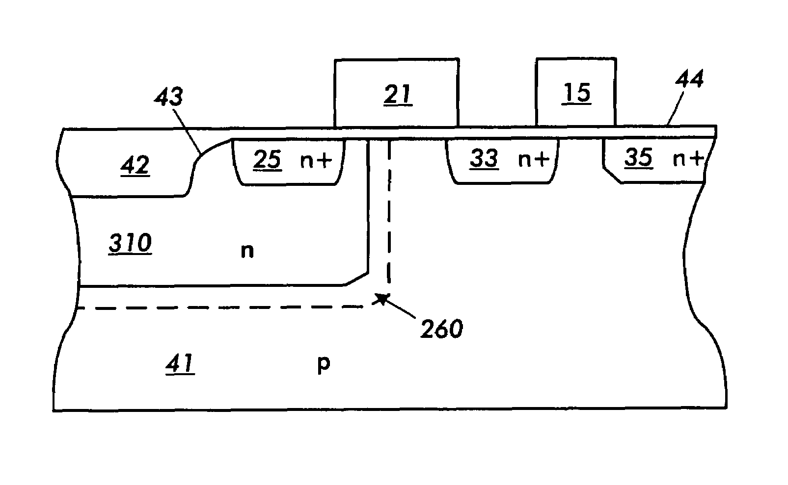
[0082]For purposes of describing the present invention, the term “well region” is being used to describe a doped substrate region i...


PUM


Abstract

A semiconductor structure, having a doped well region being formed in a substrate layer and a transistor having a terminal provided within said doped well region. The semiconductor structure also includes an oxide layer formed over the substrate layer, the doped well region, a poly silicon region, and the terminal of the transistor. The oxide layer including a step region being located where a height of the oxide layer transitions from a height associated with the doped well region to a height associated with the terminal of the transistor.

Description

REFERENCE TO RELATED APPLICATIONS[0001]This application is a divisional of U.S. application Ser. No. 10 / 752,845 filed Jan. 7, 2004, which claims priority under 35 U.S.C. §119(e) of U.S. Provisional Application No. 60 / 438,684 filed Jan. 8, 2003, which are hereby incorporated by reference.FIELD OF THE PRESENT INVENTION[0002]The present invention relates to imaging devices and, in particular, to complementary metal-oxide semiconductor (CMOS) image sensors having photodiodes with gated junctions to substantially reduce extraneous leakage current that induces fixed pattern and random noise.BACKGROUND OF THE PRESENT INVENTION[0003]CMOS image sensors are attractive for use in, e.g., still and video imaging applications, due to their compatibility with VLSI circuit design and fabrication processing. For many applications, a CMOS imager can be preferred over a corresponding CCD imager. Specifically, low-cost, large-scale CMOS design and fabrication technologies that have been developed for l...

Claims


Application Information

Patent Timeline
Patent Type & Authority Patents(United States)
IPC IPC(8): H01L31/0328
CPCH01L27/14603
Inventor DROWLEY, CLIFFORD I.WANG, CHING-CHUNYANG, JUNGWOOK
Owner SEMICON COMPONENTS IND LLC
Why Eureka
Try Eureka