Magnetically directed self-assembly of molecular electronic junctions comprising conductively coated ferromagnetic microparticles

Inactive Publication Date: 2008-01-15
THE UNITED STATES OF AMERICA AS REPRESENTED BY THE SECRETARY OF THE NAVY
View PDF4 Cites 7 Cited by
  • Summary
  • Abstract
  • Description
  • Claims
  • Application Information

AI Technical Summary

Problems solved by technology

A formidable challenge to the realization of molecular electronics is the development of high-throughput techniques for assembling nanoelectronic devices on a scale competitive with established complementary metal-oxide-semiconductor (CMOS) processes.

Method used


Image

  • Magnetically directed self-assembly of molecular electronic junctions comprising conductively coated ferromagnetic microparticles
  • Magnetically directed self-assembly of molecular electronic junctions comprising conductively coated ferromagnetic microparticles
  • Magnetically directed self-assembly of molecular electronic junctions comprising conductively coated ferromagnetic microparticles

Examples


example 1

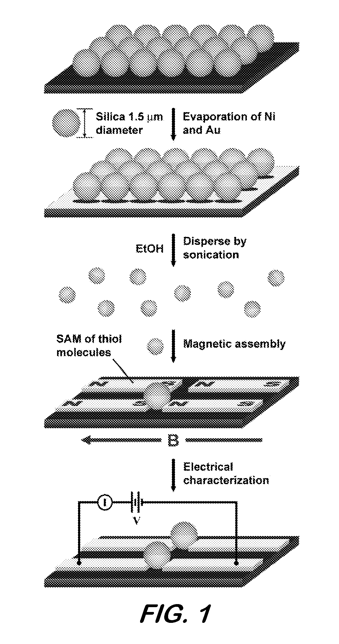
[0034]Formation of microspheres—2-D close-packed hexagonal monolayers of 1.5 micron silica beads were formed on 100 mm diameter silicon wafers by the slow evaporation of an ethanol dispersion of the colloid (Bangs Laboratories). Three prepared wafers were mounted simultaneously in an evaporative metallization chamber. 50 nm of nickel was deposited evenly on all wafers followed by 10 nm of gold. Following metallization, 100 mL of absolute ethanol was placed in a large beaker and the prepared wafers were added individually. Mild sonication for 20 min in a bath sonicator completely removed all metallized beads from the silicon surface creating a dark grey ethanol dispersion of the beads. All three wafers were stripped of their beads using the same dispersion. This concentrated “stock” solution was sonicated for another 20 minutes followed by removal of 0.5 mL of the dark dispersion. This aliquot was diluted to 100 mL with ethanol and again sonicated for 30 minutes. Approximately 10 mL ...

example 2

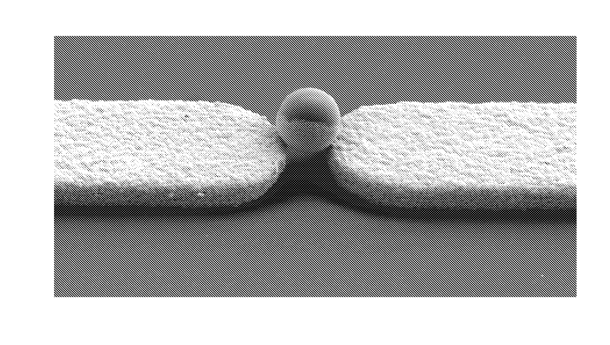
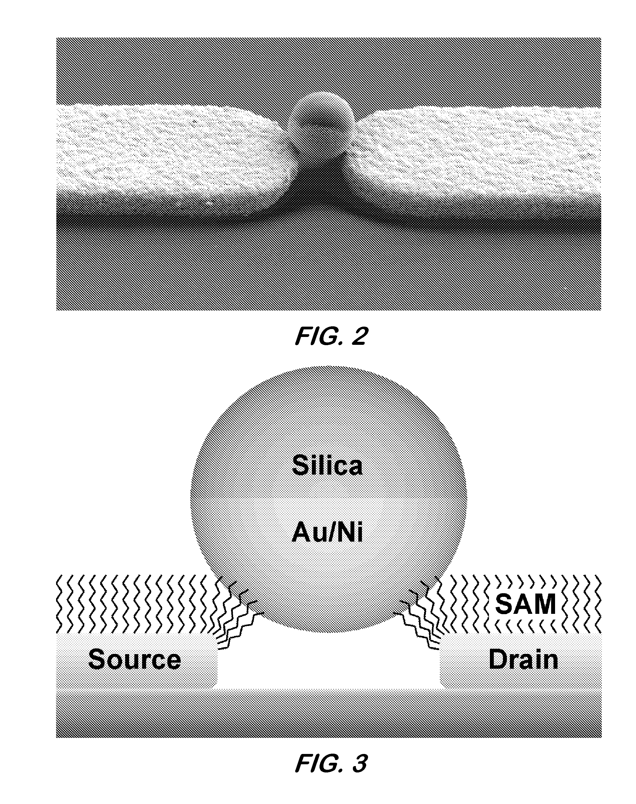
[0036]Magnetic self-assembly—The magnetic self-assembly of metallized colloid was conducted using arrays of high-aspect ratio devices composed of electroplated permalloy metal (Ni80Fe20), the fabrication of which is described in Long et al., Adv. Mater., 16, 814 (2004). Features were encased in a thin layer of electroless gold to permit thiol monolayer formation on the surface of the electrodes. Each device incorporated a set of probe tips separated by a 1 μm gap where a locally intense magnetic field would direct entrapment of the microspheres. The specific combination of a 1 μm gap width and 1.5 μm diameter colloid was carefully chosen to prevent the spheres from fitting properly in the gaps. This forces electrical contact to be made further into the metallized region of the sphere where the deposited Ni / Au film is more continuous.

[0037]Approximately 3 ml of freshly sonicated microsphere dispersion was placed in a small test tube. The test tube was then placed in a 100 Gauss magne...

example 3

[0039]Current-voltage analysis—Room temperature current-voltage (I-V) analysis was conducted on non-functionalized microsphere junctions to determine the electrical properties of the metal-metal contacts generated using this technique. Improper bead orientation after trapping prevents electrical current through the device, however the majority of trapped beads display a preferred magnetic orientation which promotes electrical contact. Proper alignment of the colloid completes the circuit across the probe tips. I-V analysis of several such junctions revealed contact resistance from 100-600 Ω, similar to reports of assembled metallic nanowires. The instrument compliance was set at 1 μA. The range of microsphere junction resistance is thought to be due to the exact positioning of the sphere and its manner of contact with the electrodes. Electrical contacts made near the edge of the metallized and silica regions were found to be of higher resistance due to lower thickness of the deposit...


PUM

PropertyMeasurementUnit
diameteraaaaaaaaaa
diameteraaaaaaaaaa
diameteraaaaaaaaaa

Abstract

A device having a substrate, a pair of ferromagnetic leads on a surface of the substrate, laterally separated by a gap, and one or more ferromagnetic microparticles comprising a conductive coating at least partially within the gap. The conductive coating forms at least part of an electrical connection between the leads. A molecular junction may connect the leads to the microparticle.

Description

BACKGROUND OF THE INVENTION[0001]1. Field of the Invention[0002]The invention relates generally to a molecular electronic junction.[0003]2. Description of the Prior Art[0004]Electronic devices based on the electronic characteristics of small assemblies of active molecules (commonly referred to as molecular electronics) have the potential of exceeding the expected scaling limits foreseen by many as a looming barrier to Moore's Law.[0005]A formidable challenge to the realization of molecular electronics is the development of high-throughput techniques for assembling nanoelectronic devices on a scale competitive with established complementary metal-oxide-semiconductor (CMOS) processes. Also needed are reliable methods capable of addressing each nanoscale unit with electrodes in such a way as to not alter or damage the active species during the assembly process. Therefore, an important step towards practical molecular electronic device fabrication is the development of a “soft” self-ass...

Claims


Application Information

Patent Timeline
Patent Type & Authority Patents(United States)
IPC IPC(8): H01F3/10B32B5/16H01L35/04H01L35/10
CPCB82Y10/00B82Y30/00B82Y40/00H01F1/14733H01L51/0508H01L51/0595B82Y25/00Y10T428/24917H01F41/26H01L2224/95085H01L2224/95144H01L2924/01079Y10T428/12153Y10T428/2991Y10T428/2993Y10T428/2995Y10T428/2989H10K10/46H10K10/701
Inventor LONG, DAVID P.KUSHMERICK, JAMES G.
Owner THE UNITED STATES OF AMERICA AS REPRESENTED BY THE SECRETARY OF THE NAVY
Why Eureka
Try Eureka