High-resolution optical channel for non-destructive navigation and processing of integrated circuits

a technology of integrated circuits and optical channels, which is applied in the direction of material analysis using wave/particle radiation, instruments, nuclear engineering, etc., can solve the problems of unfavorable optical index of mask features, damage to interlevel dielectric materials, and serious difficulties in chip and mask repair recently encountered, and achieves convenient installation, compact and lightweight, and the effect of reducing the number of components

Inactive Publication Date: 2008-04-01
GLOBALFOUNDRIES INC
View PDF2 Cites 11 Cited by
  • Summary
  • Abstract
  • Description
  • Claims
  • Application Information

AI Technical Summary

Benefits of technology

[0010]The present invention addresses the above-described need by providing an optical-fiber based light channel system included in the ion / electron beam tool (FIB or SEM). The optical channel system includes an image collection portion, an optical fiber image transmission portion and a detector portion. The image collection portion includes micro-optical components and has submillimeter dimensions, so that it is easily accommodated within the working distance of the ion / electron beam tool (that is, within about 5 mm from the workpiece). The entire system is sufficiently compact and lightweight so that it may easily be mounted on a translation stage inside the sample chamber, which permits the optical channel to be mechanically extended and retracted to avoid blocking the primary ion or electron beam. The system may be mounted to a translation stage or to a gas injector assembly, which may itself be mounted to a flange plate on the chamber wall with feed-through ports for electrical and optical signals.

Problems solved by technology

Serious difficulties in chip and mask repair have recently been encountered due to the introduction of new materials and structures that are not compatible with conventional FIB processes.
In addition, imaging the chip surface with FIB or SEM (electron beams) during navigation to the repair site can result in damage to the interlevel dielectric material.
Similarly, exposure to an ion beam in a mask repair process may lead to undesired changes in the optical index of the mask features (an effect often referred to as “staining”).
Besides materials-related issues, the constantly increasing packing density of IC features (that is, reduction in the minimum spacing between features) leads to serious problems in editing ICs and masks.
The difficulty of editing a feature without disturbing its nearest neighbors rapidly increases as the spacing between features decreases.
The minimum feature spacing is the major factor limiting the use of optical techniques for editing (e.g. laser beam based editing), due to the optical diffraction limit of spatial resolution for these techniques.
Metrology for ICs presents additional challenges.
However, damage to the original surface may occur due to exposure to the ion or electron beam before an adequate thickness of a protective layer is deposited.
The arrangement of components inside typical FIB and SEM chambers makes it difficult to view the sample being processed.
FIB and SEM chambers generally cannot accommodate a conventional optical microscope for directly viewing the sample, or for providing optical exposure to the region of the sample interacting with the beam.
Two proposed solutions to this problem are as follows: (1) A Schwartzschild reflective microscope with an infrared (IR) objective lens, built into the ion beam forming column; this type of in-situ optical microscope requires a large physical working distance, resulting in a low numerical aperture (NA) and relatively poor image resolution.
It is desirable to obtain a magnified image of the sample, but space limitations inside the FIB / SEM chamber generally require that the working distance be very small.
This in turn causes difficulties in illuminating the sample, and requires an approach different from conventional endoscopy.
This means that any off-axis illumination scheme would result in physical shadowing by the imaging objective lens.
Accordingly, lack of illumination of the sample region of interest has been one of the critical issues limiting the ability to produce magnified (e.g. >10×) images with an endoscope.
In addition, magnification after image translation is not feasible due to the intrinsic resolution loss caused by fiber-based image guides.
Resolution loss occurs in coherent fiber bundle image transmission because of the finite spacing achievable between pixel elements.
In the case of single fiber-based gradient index (GRIN) image guides, which behave as a train of convex lenses continually re-focusing light toward the optical axis, resolution is lost due to the intrinsically low NA.

Method used


Image

  • High-resolution optical channel for non-destructive navigation and processing of integrated circuits
  • High-resolution optical channel for non-destructive navigation and processing of integrated circuits
  • High-resolution optical channel for non-destructive navigation and processing of integrated circuits

Examples


Embodiment Construction

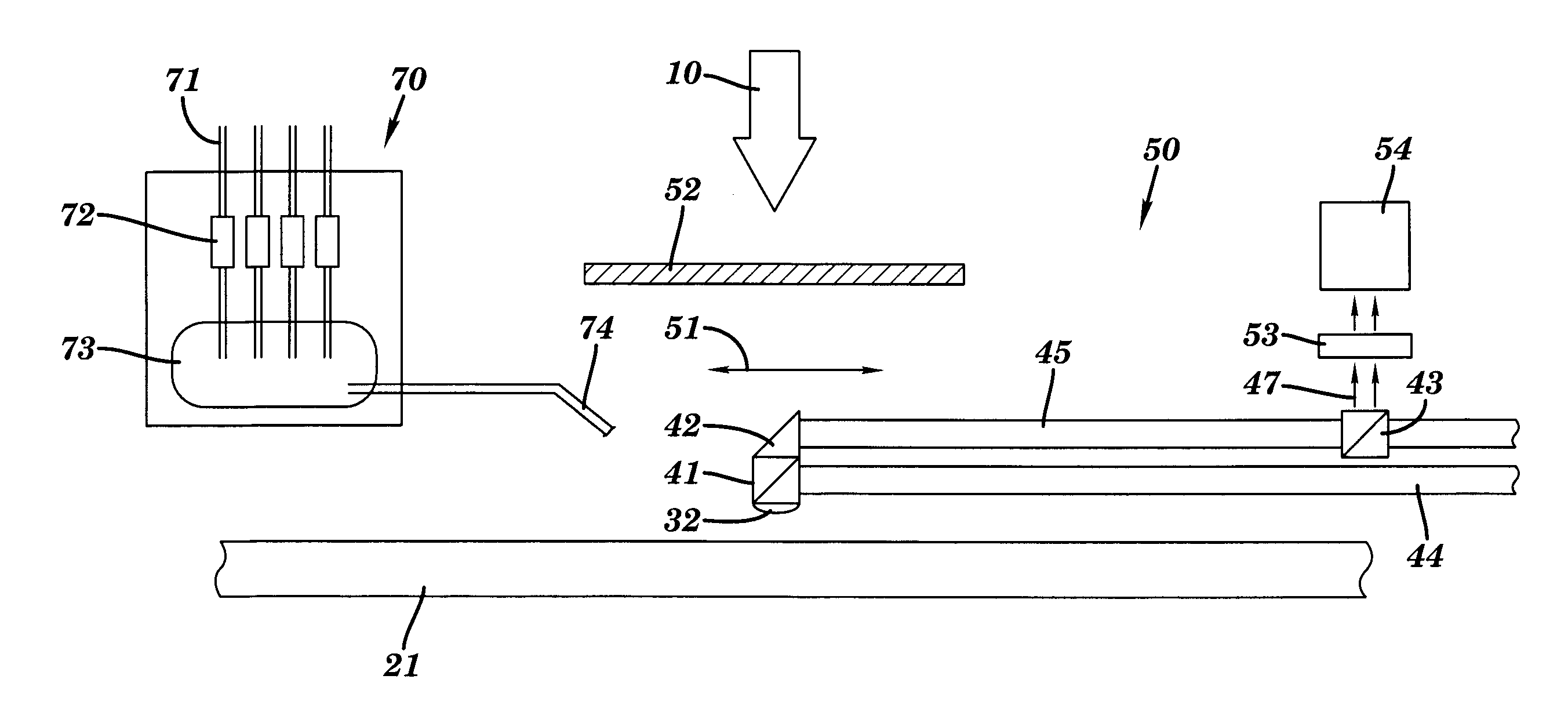
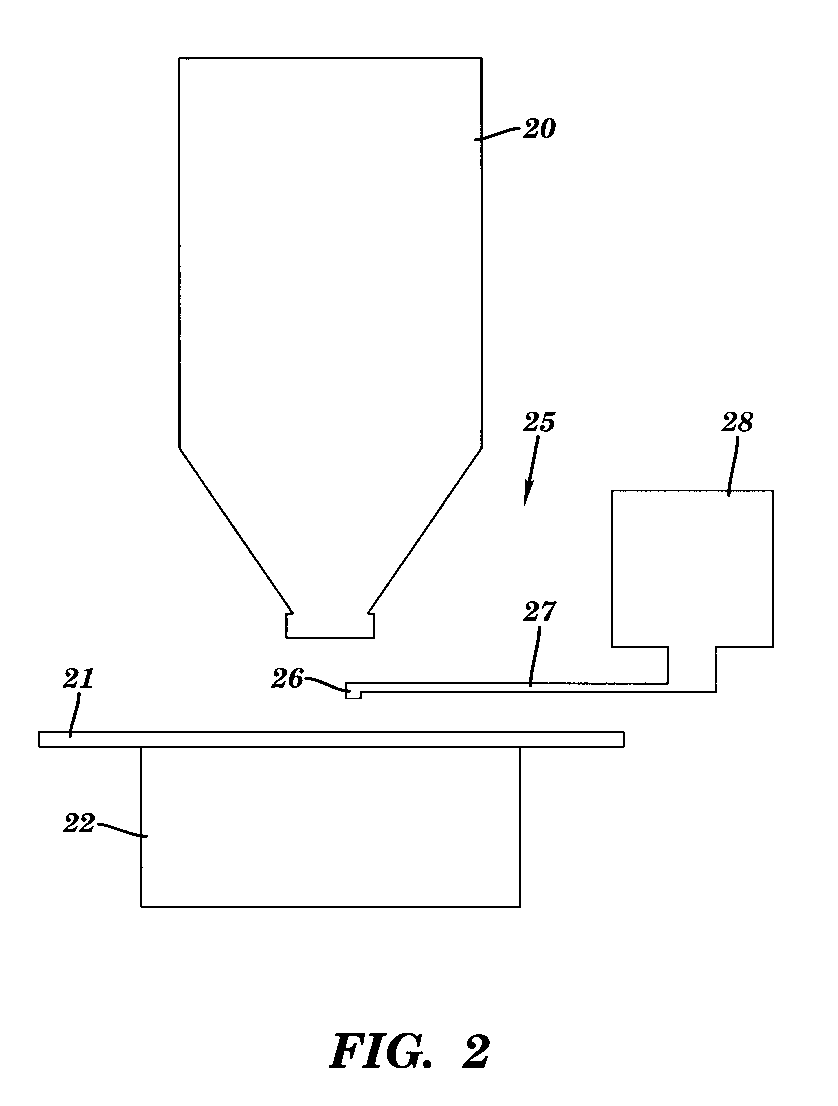
[0022]In a preferred embodiment of the invention, an optical-fiber based light channel system is included in the ion / electron beam processing tool. The interior of an FIB tool (a vacuum chamber) with a light channel system is shown in FIG. 2. Sample 21 is mounted on an XYZ motion stage 22, opposite the ion beam column 20. The optical channel system 25 includes an image collection portion 26, an optical fiber image transmission portion 27 and a detector portion 28. The image collection portion 26 includes micro-optical components (e.g. lenses and beam splitters) and has submillimeter dimensions, so that it is easily accommodated between the ion / electron column objective pole piece and the sample (i.e. within the working distance of the FIB or SEM tool). The sample 21 (typically with a repair or metrology site thereon) may therefore remain in a fixed position with respect to the column 20. The entire system 25 is sufficiently compact and lightweight so that it may easily be mounted on...


PUM


Abstract

An optical-fiber based light channel system is included in an ion / electron beam tool for imaging and / or processing integrated circuits. The optical channel system includes an image collection portion, an optical fiber image transmission portion and a detector portion. The image collection portion includes micro-optical components and has submillimeter dimensions, so that it is easily accommodated within the working distance of the ion / electron beam tool. The entire system is sufficiently compact and lightweight so that it may easily be mounted on a translation stage inside the sample chamber, which permits the optical channel to be mechanically extended and retracted to avoid blocking the primary ion or electron beam. The system may be mounted to a translation stage or to a gas injector assembly, which may itself be mounted to a flange plate on the chamber wall with feed-through ports for electrical and optical signals.

Description

FIELD OF THE INVENTION[0001]This invention relates to the manufacture of advanced integrated circuits, and particularly to repair and measurement of integrated circuits in focused-ion-beam (FIB) tools, scanning electron microscopes (SEMs), and similar environments.BACKGROUND OF THE INVENTION[0002]Current repair processes for integrated circuit (IC) chips and for lithographic exposure reticles (i.e. masks) generally rely on formation of highly localized areas of energy on the surfaces thereof, to induce spatially confined endothermic reactions for selective etching or deposition of materials. Focused beams of ions, electrons or photons are used to form these localized areas. Focused ion beams (FIBs) have been shown to have superior process confinement and reaction rates compared to focused electron beams (e.g. in SEMs) or laser beams. FIB tools have thus assumed a dominant role in most repair applications, as well as for site-specific cross-sectioning in the failure analysis of ICs.[...

Claims


Application Information

Patent Timeline
Patent Type & Authority Patents(United States)
IPC IPC(8): H01J37/244
CPCH01J37/226H01J37/28H01J37/3056H01J2237/2446H01J2237/24578H01J2237/31749
Inventor MARCHMAN, HERSCHEL M.HERSCHBEIN, STEVEN B.RUE, CHADRENNER, MICHAELRANA, NARENDER
Owner GLOBALFOUNDRIES INC
Why Eureka
Try Eureka