
Developer-soluble materials and methods of using the same in via-first dual damascene applications

a technology of development-soluble materials and damascenes, applied in the field of new dual damascene methods, can solve the problems of reducing manufacturing complexity and cost, reducing patterning and etching processes, and more complex integrated circuit devices, so as to reduce fencing or crown formation, low bias, and poor etch selectivity

Active Publication Date: 2008-04-29
BREWER SCI
View PDF106 Cites 21 Cited by
  • Summary
  • Abstract
  • Description
  • Claims
  • Application Information

AI Technical Summary

Benefits of technology

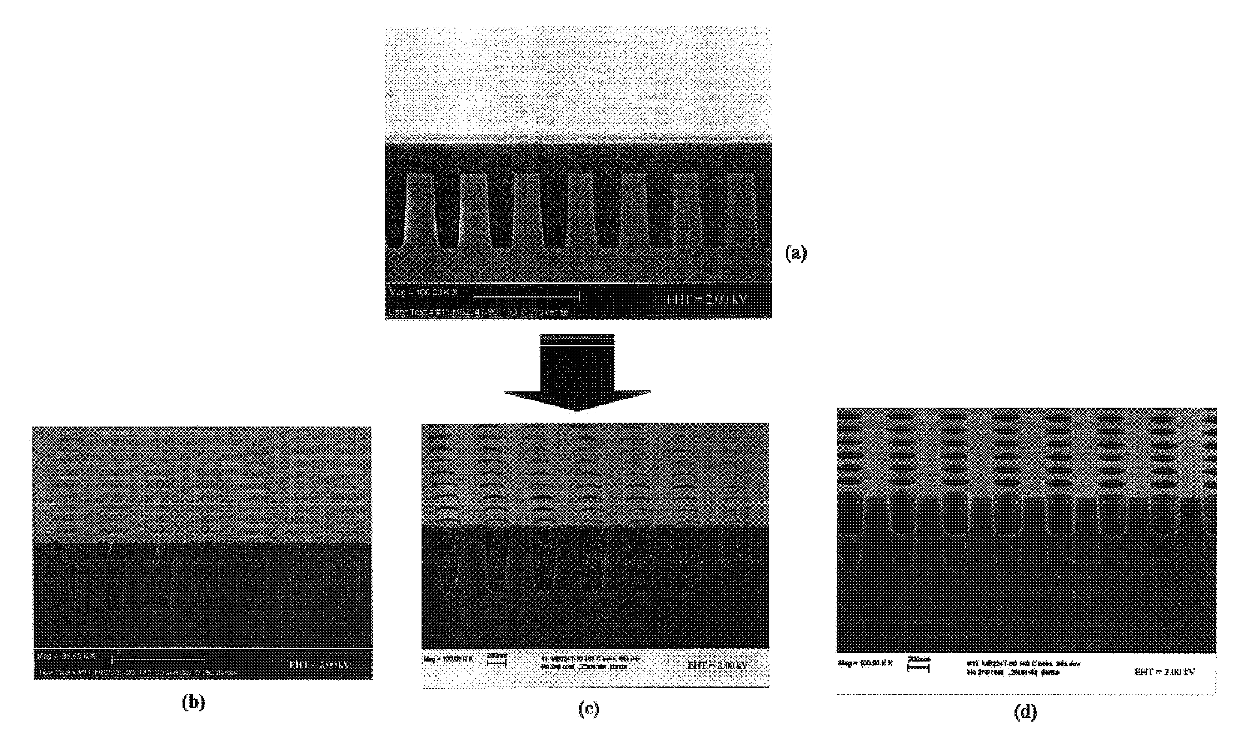
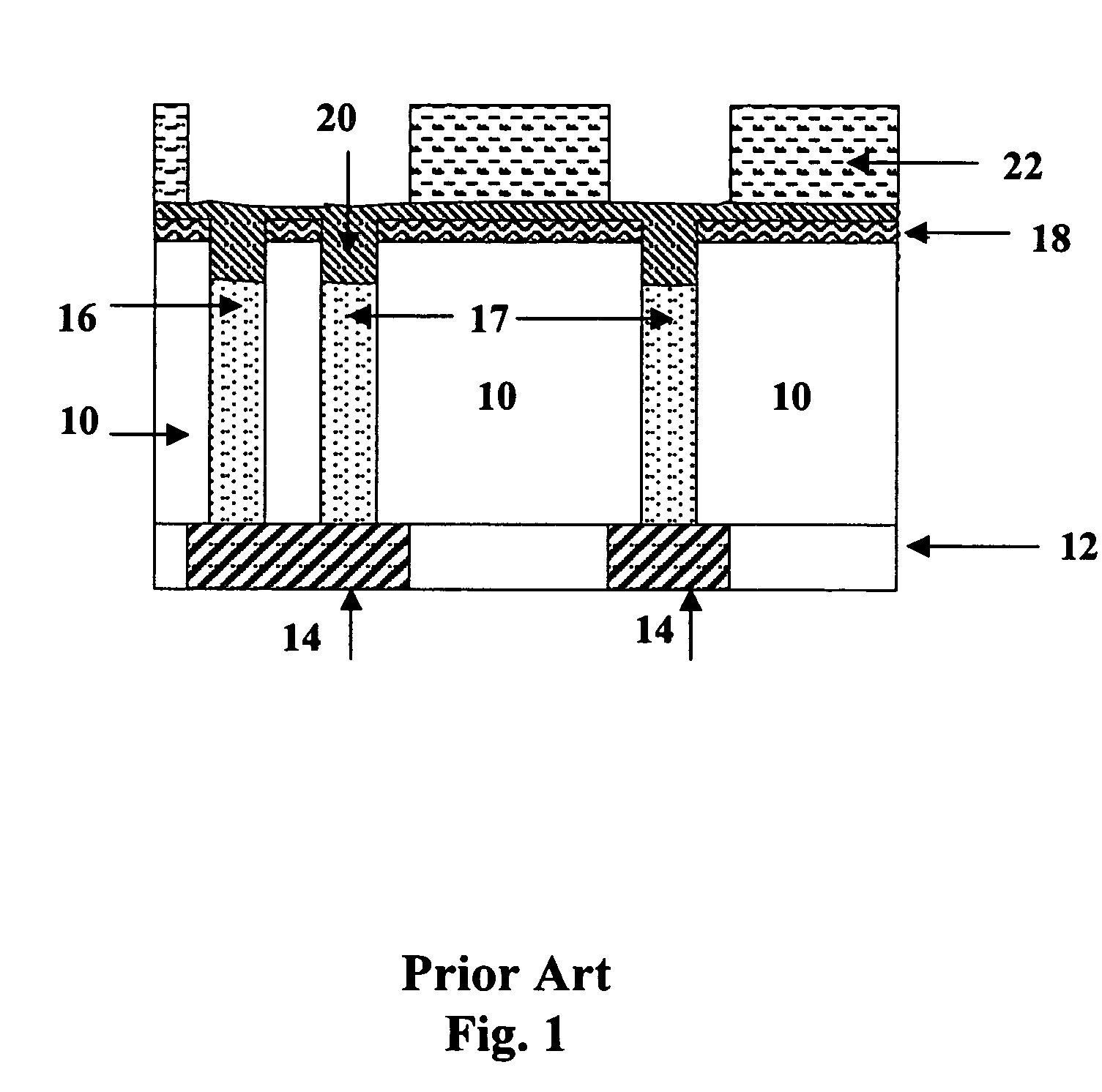
[0040]When comparing the thickness of the layer prior to developer contact to the thickness of the layer after developer contact, it can be seen that the developer contact step results in the composition being at least partially removed. Preferably, the developer contact step removes or recesses the composition at a rate of from about 1-500 Å of thickness per second of developer contact, more preferably from about 10-300 Å of thickness per second of developer contact, and even more preferably from about 20-200 Å of thickness per second of developer contact. The amount of recess can be to a level above, at, or below the upper edge of the vias, depending upon the application. If the material is recessed to a point above the upper edge of the vias, the remaining film can be used as an anti-reflective layer at its first or second reflective minimum thickness. If the material is recessed to a level at or below the upper edge of the vias, the material will act only as a gap-filling material, and another anti-reflective coating layer is preferably applied to suppress light reflecting from the substrate. Having the material recessed to partially fill the vias can be advantageous because less bottom anti-reflective coating must be etched. Minimization of the material that must be etched in the vias results in reduced fencing or crown formation after trench etch. Fences or crowns are bottom anti-reflective coating or dielectric residue that remains after the trench etch because of poor etch selectivity between the via-fill, bottom anti-reflective coating and the interlayer dielectric.
[0041]The inventive process can be used in both partial fill (i.e., where about 35-65% of the hole's depth is filled with the composition) and full-fill (i.e., where at least about 95%, and preferably about 100% of the hole's depth is filled with the composition) applications. Furthermore, it will be appreciated that the inventive methods can be used to form dual damascene structures possessing properties not previously achieved. For example, the structures prepared according to the inventive methods will have low biases, even with very thin layers of the composition. Specifically, the inventive methods will result in layers having biases of less than about 20 nm, preferably less than about 10 nm, and more preferably from about 0-5 nm, even at average film thicknesses of less than about 200 nm.

Problems solved by technology

Dual damascene processes involve fewer steps, resulting in smaller, more complex integrated circuit devices, thus lowering manufacturing complexity and cost.
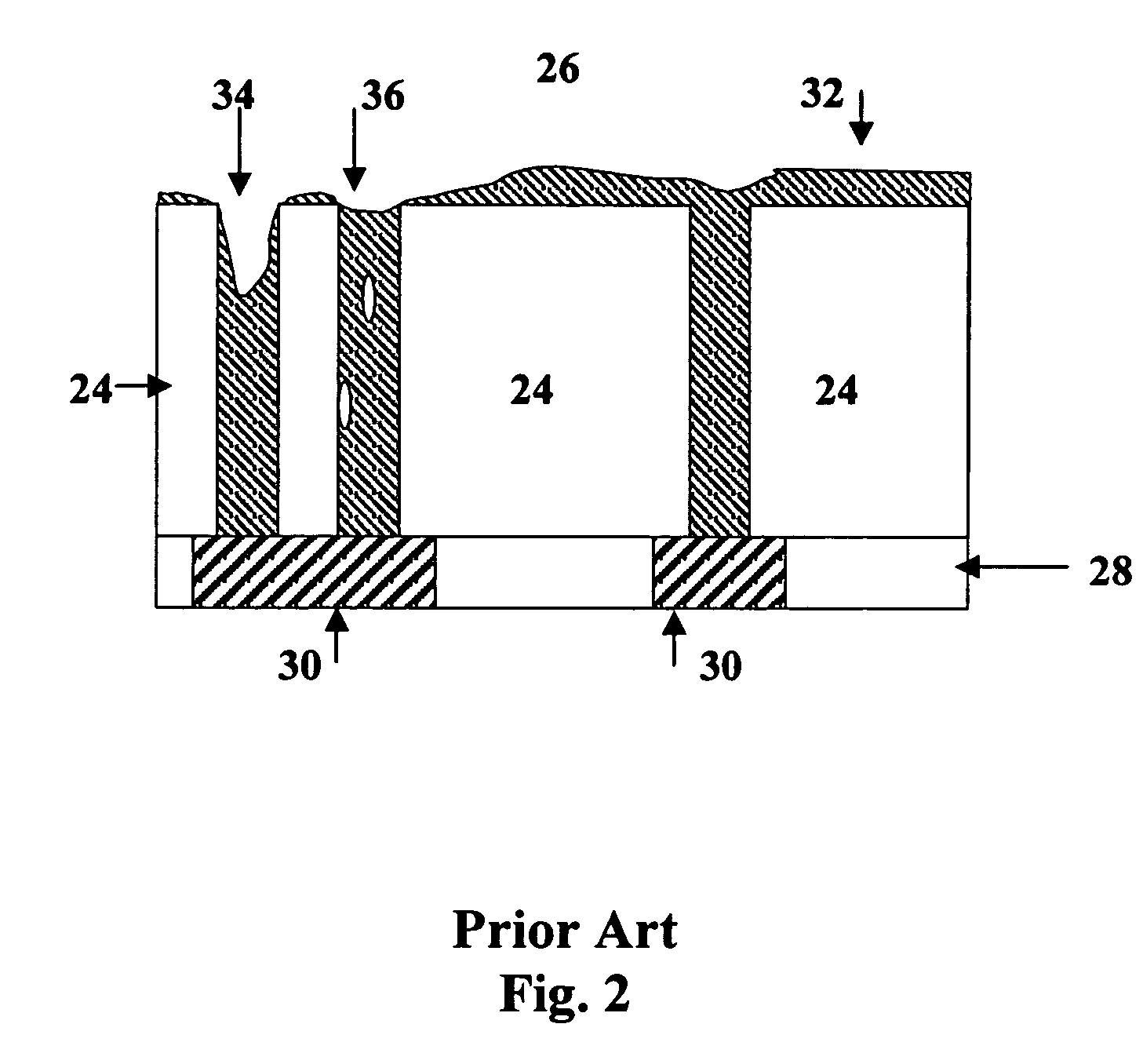
Despite the advantages of dual damascene processes, patterning and etch processes are made more difficult because of feature topography and more complex stack layers.
The application of self-aligned dual damascene is limited, because it requires a thick, intermediate layer to act as an anti-reflective layer, nearly perfect trench and via alignment, and very high etch selectivity between the dielectric and etch-stop layers.
The use of etch-stop layers may also increase the dielectric constant of the dielectric material, possibly leading to device failure.
These extra layers complicate the process and increase manufacturing costs.
Using a gap-fill material with good light-absorption and planarizing properties would simplify the process, but conventional organic bottom anti-reflective coatings do not display these properties.
The use of very thick bottom anti-reflective coatings addresses this problem, but requires a troublesome blanket-etch step to planarize the layer and reduce its thickness to more useful levels before the photoresist layer can be applied and patterned.
Blanket etch steps can also leave debris remaining in device features after etching steps, which can lead to poor electrical connections and device failure.
Removal of such debris may require the use of time-consuming, wet-cleaning techniques, and despite this, debris may still remain.
Thick bottom anti-reflective coatings can also result in a fence problem in trenches and vias.
The residue can cause incomplete trench etch, leading to poor device feature integrity.

Method used


Image

  • Developer-soluble materials and methods of using the same in via-first dual damascene applications
  • Developer-soluble materials and methods of using the same in via-first dual damascene applications
  • Developer-soluble materials and methods of using the same in via-first dual damascene applications

Examples


example 1

Preparation of Slower-Developing, Acetal Photoresist-Compatible Composition

[0064]The composition of this example was made by mixing the following ingredients together:[0065]55.0 g of the polymer solution prepared above (5.5 g polymer solids and 49.5 g PGME);[0066]16.5 g of the dye solution prepared above (3.3 g dye solids and 13.2 g PGME);[0067]1.67 g of MY720 (Ciba-Geigy);[0068]21.57 g of PGME; and[0069]36.12 g of PGMEA.

[0070]The total weight of the composition mixture was 130.86 g, with 8% solids.

[0071]The composition was spin applied at 1,500 rpm for 60 seconds onto silicon wafers and then baked at 175° C. for 60 seconds using a proximity bake plate. The film thickness of the coating was measured using an ellipsometer. The thickness range was from 290 to 300 nm across a 200-mm silicon wafer. The optical properties (n and k values) were determined using a J. A. Woollam variable angle spectroscopic ellipsometer (VASE). The optical properties of the film at a wavelength of 248 nm we...

example 2

Preparation of Faster-Developing, ESCAP Photoresist-Compatible Composition

[0076]This composition was prepared by mixing the following ingredients:[0077]24.0 g of the polymer solution prepared above (2.4 g of polymer solids, 21.6 g of PGME);[0078]7.20 g of dye solution (1.44 g of solids, 5.76 g of PGME);[0079]0.72 g of triepoxy propyl cyanurate (30% of polymer solids);[0080]9.34 g of PGME; and[0081]15.73 g of PGMEA.

[0082]The total weight of composition was 57.0 g, with 8% solids.

[0083]The composition was then spin coated, processed, and examined using the same methods described in Example 1. A proximity bake plate was used to bake the wafers.

example 3

Preparation of Faster-Developing, ESCAP Photoresist-Compatible Composition

[0084]This composition was prepared by mixing the following ingredients:[0085]12.0 g of the polymer solution prepared above (1.2 g of polymer solids, 10.8 g of PGME);[0086]7.20 g of the dye solution prepared above (1.44 g of solids, 5.76 g of PGME);[0087]0.4 g of CY179MA (33% of polymer solids; obtained from Vantico);[0088]7.64 g of PGME; and[0089]10.76 g of PGMEA.

[0090]The total weight of the composition was 38.0 g, with 8% solids.

[0091]The composition was then spin coated, processed, and examined using the same methods described in Example 1. A proximity bake plate was used to bake the wafers.

Optical Properties for Compositions of Examples 1-3

[0092]Tables I sets forth the n and k values at 193- and 248-nm wavelengths for the compositions described in Examples 1-3 above.

[0093]

TABLE IExamplen (193 nm)k (193 nm)n (248 nm)k (248 nm)11.450.451.760.4221.460.471.730.431.450.441.750.43


PUM

PropertyMeasurementUnit
time periodaaaaaaaaaa
temperatureaaaaaaaaaa
time periodaaaaaaaaaa

Abstract

Wet-recess (develop) gap-fill and bottom anti-reflective coatings based on a polyamic acid or polyester platform are provided. The polyamic acid platform allows imidization to form a polyimide when supplied with thermal energy. The gap-fill and bottom anti-reflective coatings are soluble in standard aqueous developers, and are useful for patterning via holes and trenches on semiconductor substrates in a dual damascene patterning scheme. In one embodiment, compositions composed of polyamic acids can be used as gap-filling (via-filling) materials having no anti-reflective function in a copper dual damascene process to improve iso-dense fill bias across different via arrays. In another embodiment, the same composition can be used for anti-reflective purposes, wherein the photoresist can be directly coated over the recessed surface, while it also acts as a fill material to planarize via holes on the substrate. The compositions described here are particularly suitable for use at exposure wavelengths of less than about 370 nm.

Description

RELATED APPLICATIONS[0001]This application claims the priority benefit of a provisional application entitled WET-DEVELOP (RECESS) MATERIALS BASED ON POLYAMIC ACIDS FOR VIA-FIRST DUAL DAMASCENE APPLICATIONS, Ser. No. 60 / 511,762, filed Oct. 15, 2003, incorporated by reference herein.BACKGROUND OF THE INVENTION[0002]1. Field of the Invention[0003]The present invention is concerned with new dual damascene methods utilizing a developer solution contact step after baking of a gap-fill or anti-reflective composition and prior to application of a photoresist layer. These methods result in cured layers having low biases, even on highly topographic surfaces.[0004]2. Description of the Prior Art[0005]As integrated circuit devices grow smaller, there is an increasing need for multi-level interconnects of smaller size and improved feature integrity. The damascene integration scheme is one way to allow for increasing chip densities on a substrate as design rules continue to shrink integrated circ...

Claims


Application Information

Patent Timeline
Patent Type & Authority Patents(United States)
IPC IPC(8): G03C5/00G03F7/00H01LH01L21/4763
CPCG03F7/091H01L21/76808H01L21/312H01L21/02118H01L21/28
Inventor BHAVE, MANDARWASHBURN, CARLTON A.PULIGADDA, RAMAEDWARDS, KEVIN
Owner BREWER SCI
Learn More