Carbon fine particle structure and process for producing the same, carbon fine particle transcriptional body for producing the same, solution for producing carbon fine particle structure, carbon fine particle structure, electronic device using carbon fine particle structure and process for producing the same, and integrated circuit

a technology of carbon fine particles and transcriptional bodies, applied in the direction of carbon fine particle structure, electronic devices using carbon fine particle structure and process for producing the same, etc., can solve the problems of limited cost and capability of semiconductor devices obtained through the device production process using substrate materials, the particle diameter of carbon fine particle materials cannot be increased, etc., to achieve high capability, large area, and high usefulness

Inactive Publication Date: 2008-05-06
FUJIFILM BUSINESS INNOVATION CORP
View PDF10 Cites 15 Cited by
  • Summary
  • Abstract
  • Description
  • Claims
  • Application Information

AI Technical Summary

Benefits of technology

[0015]The invention also provides materials suitable for producing the aforementioned carbon fine particle structure having high usefulness, specifically, to provide a carbon fine particle transcriptional body and a solution for producing a carbon fine particle structure.
[0016]The invention further provides an electronic device (carbon fine particle structure electronic device) with high capability and a large area capable of being produced in a convenient process by using the aforementioned carbon fine particle structure having high usefulness; and an integrated circuit obtained by integrating the aforementioned electronic devices having high capability.

Problems solved by technology

However, the particle diameter of the carbon fine particle material cannot be increased from the technical and cost conditions, and the material is limited in use as a dispersed material.
However, the production of the semiconductor device generally requires a vacuum process, such as sputtering, and a high temperature process.
Accordingly, only a limited and high-cost material can be selected as a substrate, and therefore, the application of the semiconductor device obtained through the device production process using the substrate material is limited in cost and capability.
However, the production process with low temperature and low cost and the high capability are conflicting demands, and it is difficult to attain both of them simultaneously.
For example, a material exerting high capability, such as pentacene, requires production by a vapor deposition process in high vacuum, which is not desired from the standpoint of obtaining a large area and attaining a low-cost production process.
An organic semiconductor material, such as polymer compound, can be easily produced as the device with high productivity, but the sufficient capability cannot be obtained.

Method used


Image

  • Carbon fine particle structure and process for producing the same, carbon fine particle transcriptional body for producing the same, solution for producing carbon fine particle structure, carbon fine particle structure, electronic device using carbon fine particle structure and process for producing the same, and integrated circuit
  • Carbon fine particle structure and process for producing the same, carbon fine particle transcriptional body for producing the same, solution for producing carbon fine particle structure, carbon fine particle structure, electronic device using carbon fine particle structure and process for producing the same, and integrated circuit
  • Carbon fine particle structure and process for producing the same, carbon fine particle transcriptional body for producing the same, solution for producing carbon fine particle structure, carbon fine particle structure, electronic device using carbon fine particle structure and process for producing the same, and integrated circuit

Examples


specific embodiments

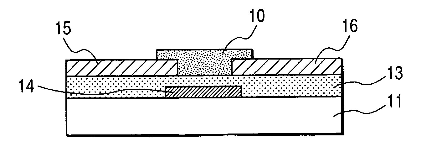
[0290]A protective layer or other functional layers may be formed as an upper layer of the carbon fine particle structure layer thus patterned. Upon forming a protective layer as an upper layer of the carbon fine particle structure layer, the carbon fine particle structure as a network obtained by crosslinking carbon fine particles can be further firmly retained on the surface of the base body and can be protected from an external force. The protective layer may be a resist layer remaining but having not been removed, which will be described for the production process of the carbon fine particle structure. It is also effective that a protective layer is newly formed to cover the entire surface including the area thus patterned to the desired shape. As the material for constituting the protective layer, various kinds of resin materials and inorganic materials having been known in the art can be used depending on purposes.

[0291]The carbon fine particle structure layers may be accumula...

application example of

(Application Example of Production Process of Electronic Device of the Invention)

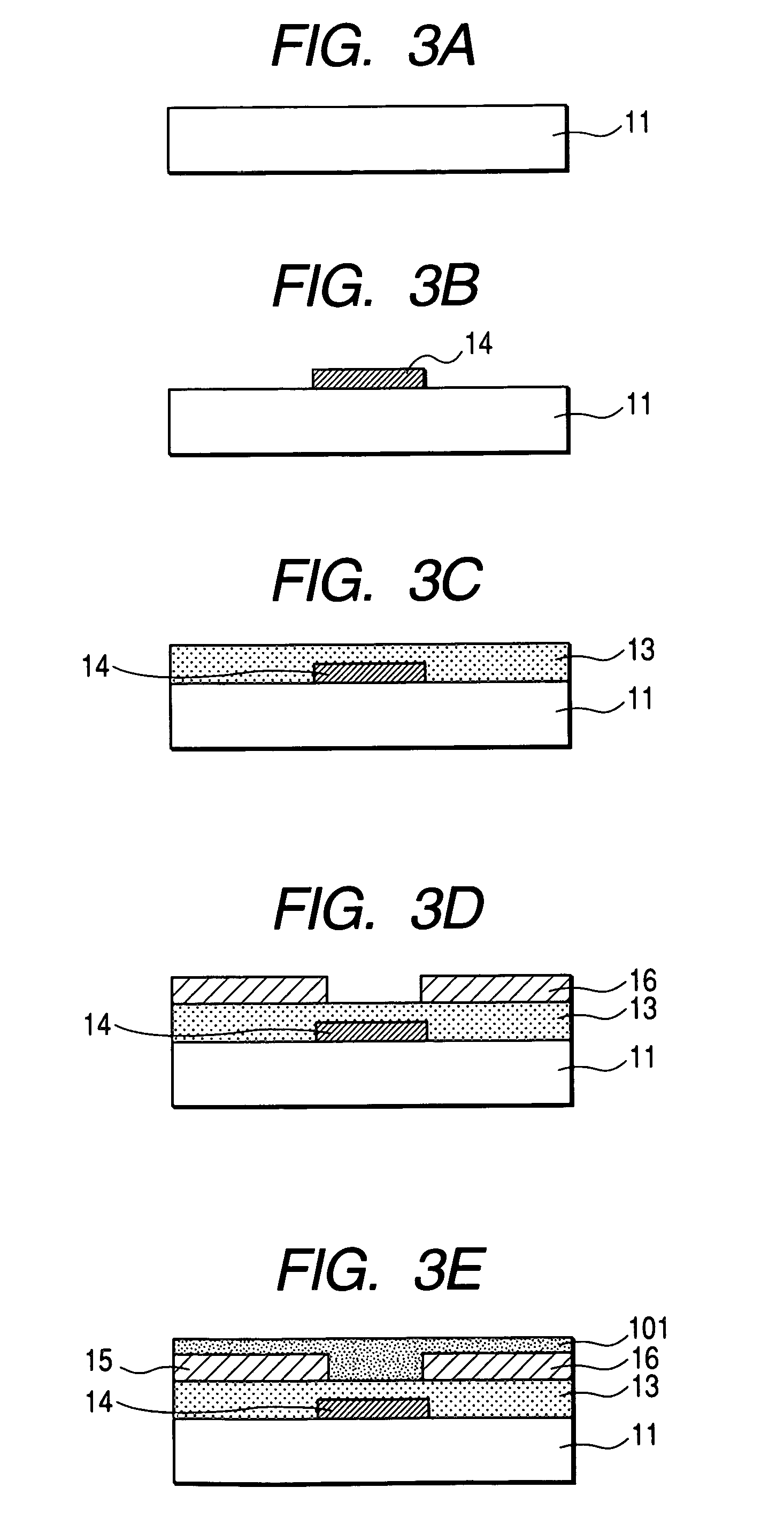
[0419]As a useful application example of the production process of an electronic device of the invention, it is possible that the carbon fine particle structure layer is once patterned on a surface of a preliminary substrate, and the layer is then transferred to the target base body. In the transferring step, it is possible that the patterned carbon fine particle structure layer is once transferred from the preliminary substrate to a surface of an intermediate transfer material, and the layer is then transferred to the target base body (second base body).

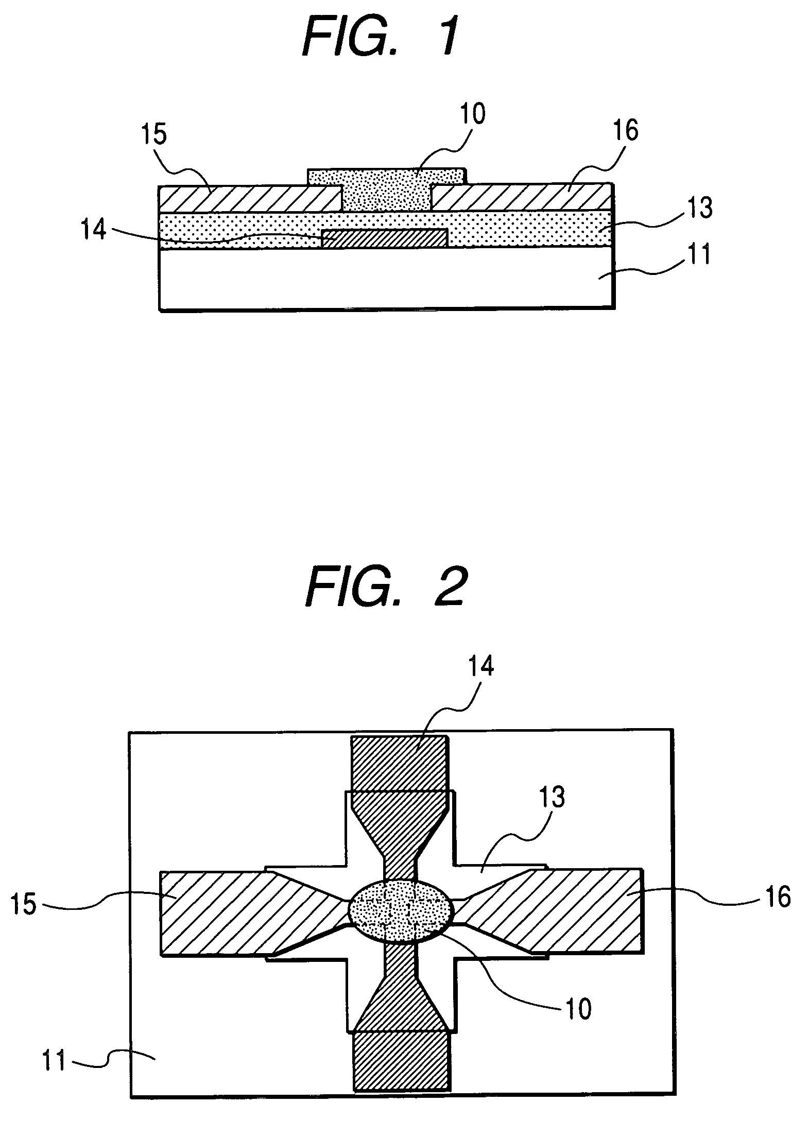
[0420]The process for producing a MOS-FET type carbon fine particle transistor as one embodiment of the electronic device of the invention will be specifically described with reference to FIGS. 5A to 5E.

[0421]A carbon fine particle structure is formed on a preliminary substrate 11′ and patterned to a shape corresponding to a transporting layer 11, in th...

example 1

[0440]A carbon fine particle structure having a carbon black-glycerol crosslinked film having semiconductor characteristics is produced by using carbon black as carbon fine particles.

(A) Applying Step

(A-1) Preparation of Crosslinking Solution (Adding Step)

(i) Addition of Carboxylic Group—Synthesis of Carbon Black Carboxylic Acid

[0441]1 g of carbon black powder (REGAL 330, a trademark, produced by Cabot Oil & Gas Corp., average particle diameter: 25 nm) is added to 50 mL of concentrated nitric acid (60% by mass aqueous solution, produced by Kanto Kagaku Co., Ltd.) and then refluxed at 120° C. for 6 hours to synthesize carbon black carboxylic acid. The reaction scheme of the reaction is shown in FIG. 6. The part of the carbon black is shown by a hollow elliptic shape in FIG. 6 (which is the same in other figures showing reaction schemes).

[0442]After the temperature of the solution is lowered to room temperature, the solution is subjected to centrifugal separation at 5,000 rpm for 15 m...


PUM

PropertyMeasurementUnit
diameteraaaaaaaaaa
particle diameteraaaaaaaaaa

Abstract

A carbon fine particle structure containing plural carbon fine particles having a graphite structure and a crosslinked part containing plural functional groups chemically bonded to each other, at least one ends of each of the functional groups being connected to different carbon fine particles, the plural carbon fine particles and the crosslinked part constituting a network structure, and a process for producing the same are provided. A carbon fine particle transcriptional body and a solution for producing the carbon fine particle structure, an carbon fine particle structure electronic device using the carbon fine particle structure and a process for producing the same, and an integrated circuit using the same are provided.

Description

BACKGROUND OF THE INVENTION[0001]1. Field of the Invention[0002]The present invention relates to a carbon fine particle structure as a useful novel substance that is obtained by structuralizing an inexpensive carbon fine particle material, such as carbon black and graphite, a process for producing the same, a carbon fine particle transcriptional body for producing the same, and a solution for producing a carbon fine particle structure.[0003]The invention also relates to a carbon fine particle structure electronic device and an integrated circuit having high usefulness using the carbon fine particle structure, and a process for producing the carbon fine particle structure electronic device.[0004]2. Description of the Related Art[0005]A carbon fine particle material, such as carbon black and graphite, has been used as a conductive paste, a pigment and a conductivity imparting agent for rubber and plastics. The carbon fine particle material is superior since it has corrosion resistance...

Claims


Application Information

Patent Timeline
Patent Type & Authority Patents(United States)
IPC IPC(8): C09C1/44C01B31/04D01F9/12C09C1/46C09C1/56
CPCC09C1/46C09C1/56C01P2006/40
Inventor OKADA, SHINSUKEHIRAKATA, MASAKIMANABE, CHIKARAANAZAWA, KAZUNORISHIGEMATSU, TAISHIWATANABE, MIHOKISHI, KENTAROUISOZAKI, TAKASHIOOMA, SHIGEKIWATANABE, HIROYUKI
Owner FUJIFILM BUSINESS INNOVATION CORP
Why Eureka
Try Eureka