Organic thin film transistor enhanced in charge carrier mobility by virtue of surface relief structure
a thin film transistor and surface relief technology, applied in transistors, solid-state devices, thermoelectric devices, etc., can solve the problems of reducing charge carrier mobility, and inferiority of organic insulating layers
- Summary
- Abstract
- Description
- Claims
- Application Information
AI Technical Summary
Benefits of technology
Problems solved by technology
Method used
Image
Examples
example 1
Formation of an Organic Insulating Layer of Surface Relief Structure
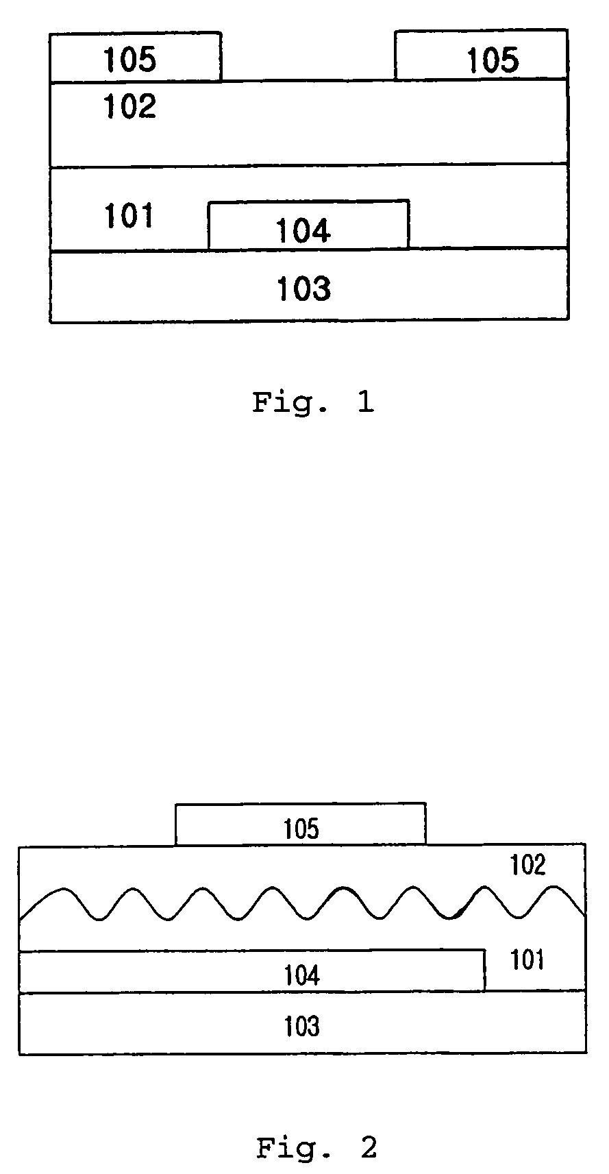
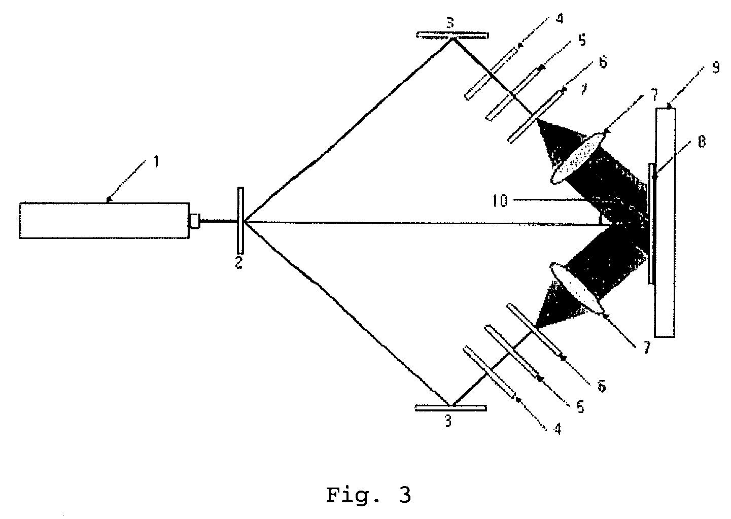
[0035]Onto a silicon substrate where a gate electrode was previously deposited, a 10 wt % solution of poly(4-nitrophenylazophenyloxylpentyl methacrylate-co-hydroxyethyl methacrylate) (Mw=35,000, MWD=2.5) in cyclohexanone was applied by spin coating to a thickness of 500 nm. The solvent was evaporated by drying the coated substrate at 100 □ for 10 minutes. The dried substrate was exposed to light having a wavelength of 488 nm by the use of a laser interferometer with an Ar+ laser. The incident angle of the laser beam was adjusted to 50° to afford a mono-axial lattice pattern having an interval period(Λ) of 500 nm and a depth of 50 nm. FIGS. 4a and 4b show AFM images of the resulting organic insulating layer.
example 2
Fabrication of an Organic TFT Device Using an Organic Insulating Layer of Surface Relief Structure
[0036]Onto the organic insulating layer of surface relief structure obtained from Example 1, a 1 wt % solution of poly(dioctylfulorene-co-bithiophene) in toluene was applied by spin coating to a thickness of 70 nm. The solvent was evaporated by drying the coated substrate at 100 □ for 30 minutes. On the resulting organic active layer were deposited source / drain electrodes by the use of a shadow mask having a channel length of 100 μm and a channel width of 2 mm to afford an organic TFT device. The direction of the channel length was equal to that of the major axis of the surface relief structure of the organic insulating layer.
example 3
Variation of the Electronic Properties of the Organic TFT Devices According to the Direction of the Surface Relief Structure
[0048]Two organic TFT devices, in which the major axis of the surface relief structure and the S-D channel were arrayed in the direction as shown in FIGS. 5a and 5b, were fabricated according to Examples 1 and 2 above. The current-transfer curves and charge carrier mobility curves of these devices were plotted in FIGS. 6 and 7, respectively. As a control, the current-transfer curve and charge carrier mobility curve of the device fabricated in the above Comparative Example were plotted simultaneously therewith.
[0049]As can be seen from FIGS. 6 and 7, device (II), in which the major axis of the surface relief structure and the S-D channel are parallel to each other, exhibited superior charge carrier mobility to the device (I), in which the major axis of the surface relief structure and the S-D channel are perpendicular to each other. On the other hand, device (I)...
PUM
| Property | Measurement | Unit |
|---|---|---|
| threshold voltage | aaaaa | aaaaa |
| threshold voltage | aaaaa | aaaaa |
| dielectric constant | aaaaa | aaaaa |
Abstract
Description
Claims
Application Information


