Crystalline III-V nitride films on refractory metal substrates

a technology of metal nitride and crystalline iii-v, which is applied in the direction of basic electric elements, electrical equipment, semiconductor devices, etc., can solve the problems of large lattice and thermal mismatch of materials

Inactive Publication Date: 2009-01-27
THE UNITED STATES OF AMERICA AS REPRESENTED BY THE SECRETARY OF THE NAVY
View PDF4 Cites 13 Cited by
  • Summary
  • Abstract
  • Description
  • Claims
  • Application Information

AI Technical Summary

Benefits of technology

[0005]The invention comprises an article of manufacture comprising: a substrate having a top surface comprising titanium carbide, vanadium carbide, zirconium carbide, niobium carbide, hafnium carbide, tantalum carbide, tungsten carbide, chromium nitride, molybdenum nitride, tungsten nitride, titanium nitride, vanadium nitride, zirconium nitride, or a combination thereof; and a first layer disposed on the top surface comprising one or more group III-V metal nitrides.
[0006]The invention further comprises a method comprising: providing a substrate having a top surface comprising titanium carbide, vanadium carbide, zirconium carbide, niobium carbide, hafnium carbide, tantalum carbide, tungsten carbide, chromium nitride, molybdenum nitride, tungsten nitride, titanium nitride, vanadium nitride, zirconium nitride, or a combination thereof; and depositing on the top surface a first layer comprising one or more group III-V metal nitrides.

Problems solved by technology

Both of these materials have large lattice and thermal mismatch with gallium nitride and its alloys.

Method used


Image

  • Crystalline III-V nitride films on refractory metal substrates
  • Crystalline III-V nitride films on refractory metal substrates
  • Crystalline III-V nitride films on refractory metal substrates

Examples


example 1

[0030]General procedure—Titanium carbide substrates were loaded into a reactor for the epitaxial growth of gallium nitride or its alloys. Organometallic vapor phase epitaxy was used for this growth. Titanium carbide substrates were heated for a cleaning step up to 1350° C. for 3 min, then cooled down to 450° C. for growth of the nucleation layer. While aluminum nitride was utilized for the nucleation layer, a gallium nitride or alloyed aluminum / gallium / indium nitride nucleation layer can be used with the same resultant effect. Triethylaluminum (200 sccm flowed through a source at 1000 torr at a constant temperature of 30° C.) and 2.5 SLM (standard liters per minute) ammonia were used as reactants in 3.5 SLM hydrogen carrier gas. Following formation of the nucleation layer, which took approximately 13 min, the temperature was raised to 1000° C. over a period of 5 min. Once 1000° C. was reached, gallium nitride growth was commenced. Trimethylgallium (20 sccm flowed through a source at...

example 2

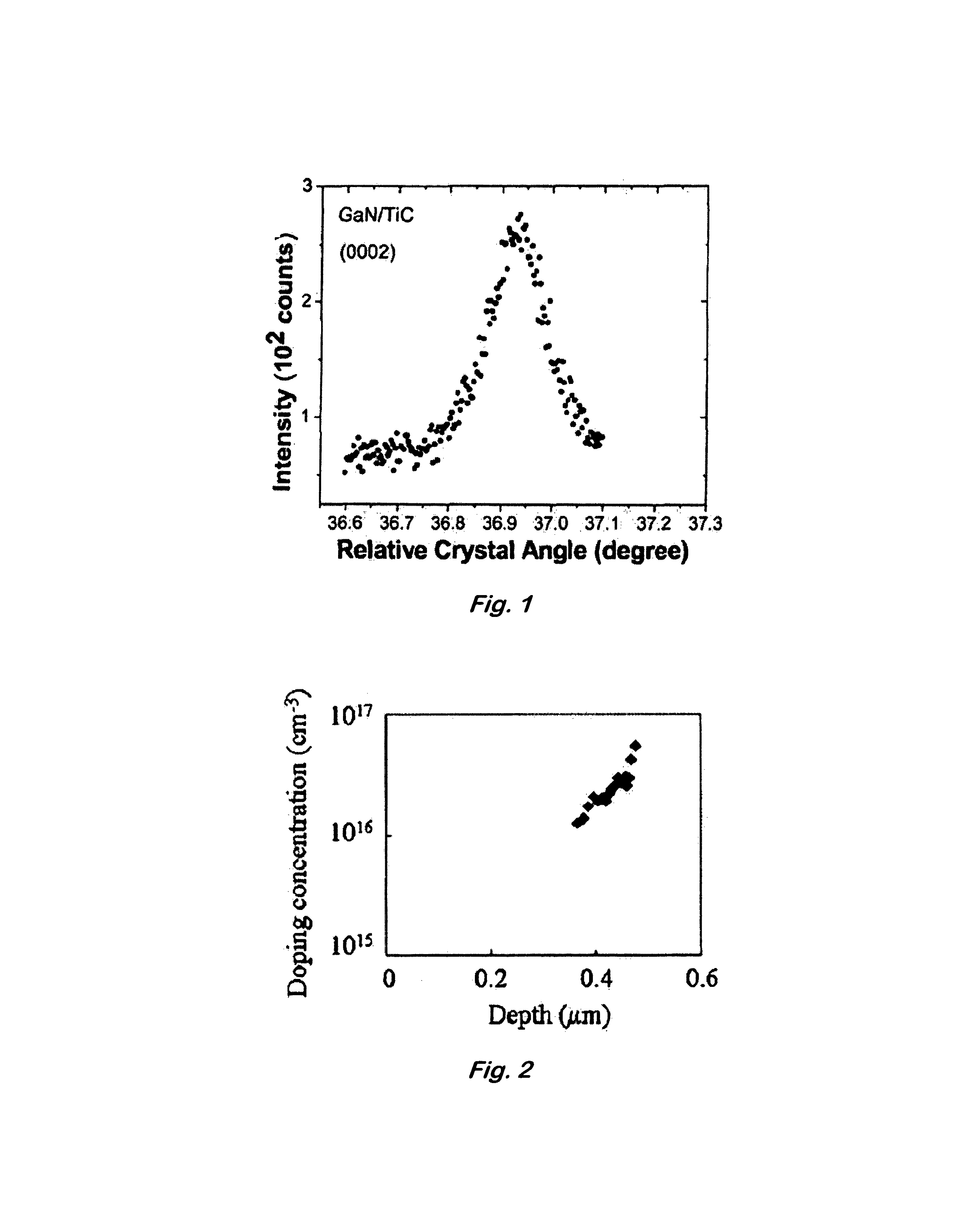
[0031]The TiC substrates used were grown by a high-pressure float-zone method (Parsons et al., Solid State Technol., 11, 133 (1990)). Epitaxial gallium nitride films of about 3.0 μm thickness were grown on both TiC (100) and (111) substrates by low-pressure organometallic vapor phase epitaxy (LP-OMVPE) in a vertical reactor geometry at 57 Torr. The surface of substrates 5 mm square and ˜1 mm in thickness were solvent-cleaned and heated to 1350° C. in H2 for 5 min prior to growth. Nucleation layers of AlN with 15 mm of thickness were then grown at 450° C. using triethylaluminum, ammonia, and hydrogen. AlN was used as the nucleation layer because its atomic spacing is intermediate to TiC and GaN and 1.5% mismatched to TiC. GaN films were then grown at 1000° C. using trimethylgallium, ammonia, and hydrogen. Films with a root-mean-square (rms) roughness of 0.55 nm (1×1 μm area) as determined by atomic force microscopy (AFM) were deposited. Submicrometer size pores, typically observed in...

example 3

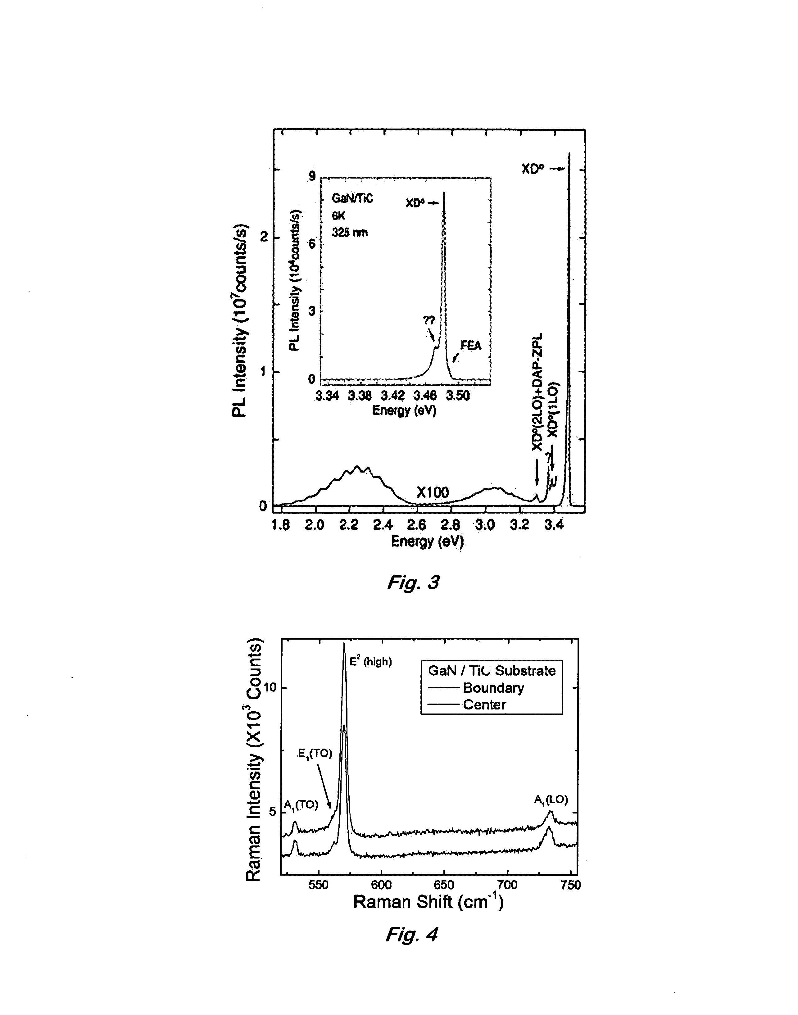
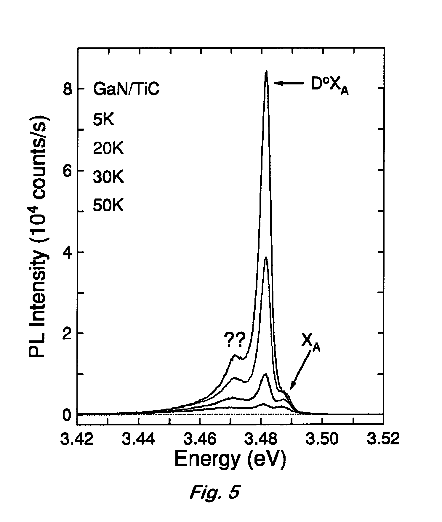
[0035]Substrates of (100) and (111) TiC, 5 mm square and ˜1.0 mm thick, were loaded into an organometallic vapor phase epitaxy reactor for the GaN epitaxial growth. TiC substrates were heated in hydrogen at 1350° C. for 3 min, then cooled down to 450° C. for growth of a nucleation layer. Aluminum nitride was utilized for the nucleation layer. A GaN or alloyed AlInGaN nucleation layer can also be used with the same result. Triethylaluminum (1.5×10⁻⁴ mol / min) and 2.5 SLM (standard liters per minute) ammonia were used as reactants in 3.5 SLM hydrogen carrier gas. Following formation of the nucleation layer, which took approximately 13 min, the temperature was raised to 1000° C. over a period of 5 min. Once 1000° C. was reached, GaN growth commenced. Trimethylgallium (4.1×10⁻⁵ mol / min) and 2.5 SLM ammonia were used as reactants in 3.5 SLM hydrogen carrier gas. Growth of the GaN took place for 85 min. All growth was carried out at a total pressure of 57 torr. Samples were cooled in 2.5 S...


PUM

PropertyMeasurementUnit
temperatureaaaaaaaaaa

Abstract

An article of manufacture having a substrate having a top surface and a first layer on the top surface. The top surface contains titanium carbide, vanadium carbide, zirconium carbide, niobium carbide, hafnium carbide, tantalum carbide, tungsten carbide, chromium nitride, molybdenum nitride, tungsten nitride, titanium nitride, vanadium nitride, zirconium nitride, or a combination thereof. The first layer contains one or more group III-V metal nitrides.

Description

FIELD OF THE INVENTION[0001]The invention is generally related to group III-V metal nitride films.DESCRIPTION OF RELATED ART[0002]The III-nitride semiconductor system possesses a unique combination of physical and chemical properties that allows the formation of alloys and heterostructures necessary for the fabrication of optical devices and electronic devices capable of operating at high power and high temperature and / or under extreme environmental conditions. Ternary or quaternary alloys of GaN, AlN, and InN have been grown to produce optical devices that emit light spanning from red to deep UV. Green, blue, near / deep-UV, and white light emitting devices, UV detectors, and near-UV lasers are presently commercially available.[0003]Current methods of obtaining high-quality gallium nitride involve primarily the use of either sapphire, which is insulating, or silicon carbide, which is a semiconductor. Both of these materials have large lattice and thermal mismatch with gallium nitride...

Claims


Application Information

Patent Timeline
Patent Type & Authority Patents(United States)
IPC IPC(8): H01L29/12H01L21/36
CPCH01L21/02425H01L21/02433H01L21/02458H01L21/0254H01L21/0262H01L29/7371H01L29/8083H01L29/868H01L29/872H01L21/0237H01L29/2003
Inventor FREITAS, JAIME A.ROWLAND, LARRY B.
Owner THE UNITED STATES OF AMERICA AS REPRESENTED BY THE SECRETARY OF THE NAVY
Why Eureka
Try Eureka