Nitride-based light-emitting device having grid cell layer

a light-emitting device and grid cell technology, applied in the direction of solid-state devices, lasers, semiconductor lasers, etc., can solve the problems of low light utilization efficiency, and inability to develop a p-ohmic electrode layer suitable for a tled or fled structure, and achieve low sheet resistance, prevent degradation of performance, and low specific ohmic contact resistance

Active Publication Date: 2009-02-03
SAMSUNG ELECTRONICS CO LTD +1
View PDF8 Cites 31 Cited by
  • Summary
  • Abstract
  • Description
  • Claims
  • Application Information

AI Technical Summary

Benefits of technology

[0022]Embodiments of the present invention provide a nitride-based light-emitting device including an ohmic contact electrode with low sheet resistance and low specific ohmic contact resistivity and a method of manufacturing the same. Embodiments of the present invention also provide a nitride-based light-emitting device fabricated using a simple process that can prevent degradation of performance caused during thin film formation and a method of manufacturing the same.
[0027]The nitride-based light-emitting device further includes an agglomeration preventing layer that is formed on the reflective ohmic contact layer and prevents damage to the reflective ohmic contact layer. It is made from at least one material selected from the group consisting of Cu, silicon (Si), germanium (Ge), Zn, Mg, Ti, tungsten (W), lithium (Li), and an alloy containing the above metals.

Problems solved by technology

However, due to an inverse relationship that most electrode materials have between optical and electrical characteristics and poor electrical characteristics such as low current injection and current spreading in a p-cladding layer, it is difficult to develop a p-ohmic electrode layer suitable for a TLED or FLED structure.
Due to their low light utilization efficiency, TLEDs using an oxidized semi-transparent Ni / Au electrode film are not suited for realizing large-capacity, high brightness light-emitting devices.
While temporarily providing high luminous efficiency, use of the highly reflective material with a low work function makes it difficult to form a p-ohmic contact electrode with low specific ohmic contact resistivity and high thermal stability.
Consequently, it is difficult to provide a long life span and high reliability of a light-emitting device.
For example, Al cannot be used for an ohmic contact because it tends to form a Schottky (non-ohmic) contact at the Al / p-GaN interface due to the low work function and strong tendency to form a nitride during annealing.
A g can be used to form an ohmic contact to a p-GaN but suffers from thermal instability and a poor mechanical adhesion with the p-GaN, thus making it difficult to ensure reliability during manufacturing and operation of the light-emitting device.
However, this approach also suffers limitations such as a short life time and low reliability of the device due to the ohmic contact structure with high specific contact resistivity.
However, the proposed structure has the problem of low performance due to non-oxidation of Ni.
However, fabrication of the p-type reflective ohmic contact layer is complicated and the p-type reflective ohmic contact layer has a low luminous efficiency due to its high specific ohmic contact resistivity.
However, with high specific contact resistivities and a large amount of heat generated during operation, many commonly-used ohmic electrodes for LDs degrade the life span and reliability of the device.
However, these metal dopants cannot serve their functions since they have a strong tendency to combine with hydrogen (H2) and form various types of complexes, which causes passivation.
Furthermore, because the p-type nitride-based semiconductor has a sheet resistance of above 104 Ω / cm2 due to its low hole concentration, it is difficult to form a good p-ohmic contact layer, thus hindering efficient hole injection and current spreading.
However, the p-ohmic contact electrode thus fabricated has insufficient specific ohmic contact resistivity and optical characteristics to realize a high quality nitride-based light-emitting device.

Method used


Image

  • Nitride-based light-emitting device having grid cell layer
  • Nitride-based light-emitting device having grid cell layer
  • Nitride-based light-emitting device having grid cell layer

Examples


first embodiment

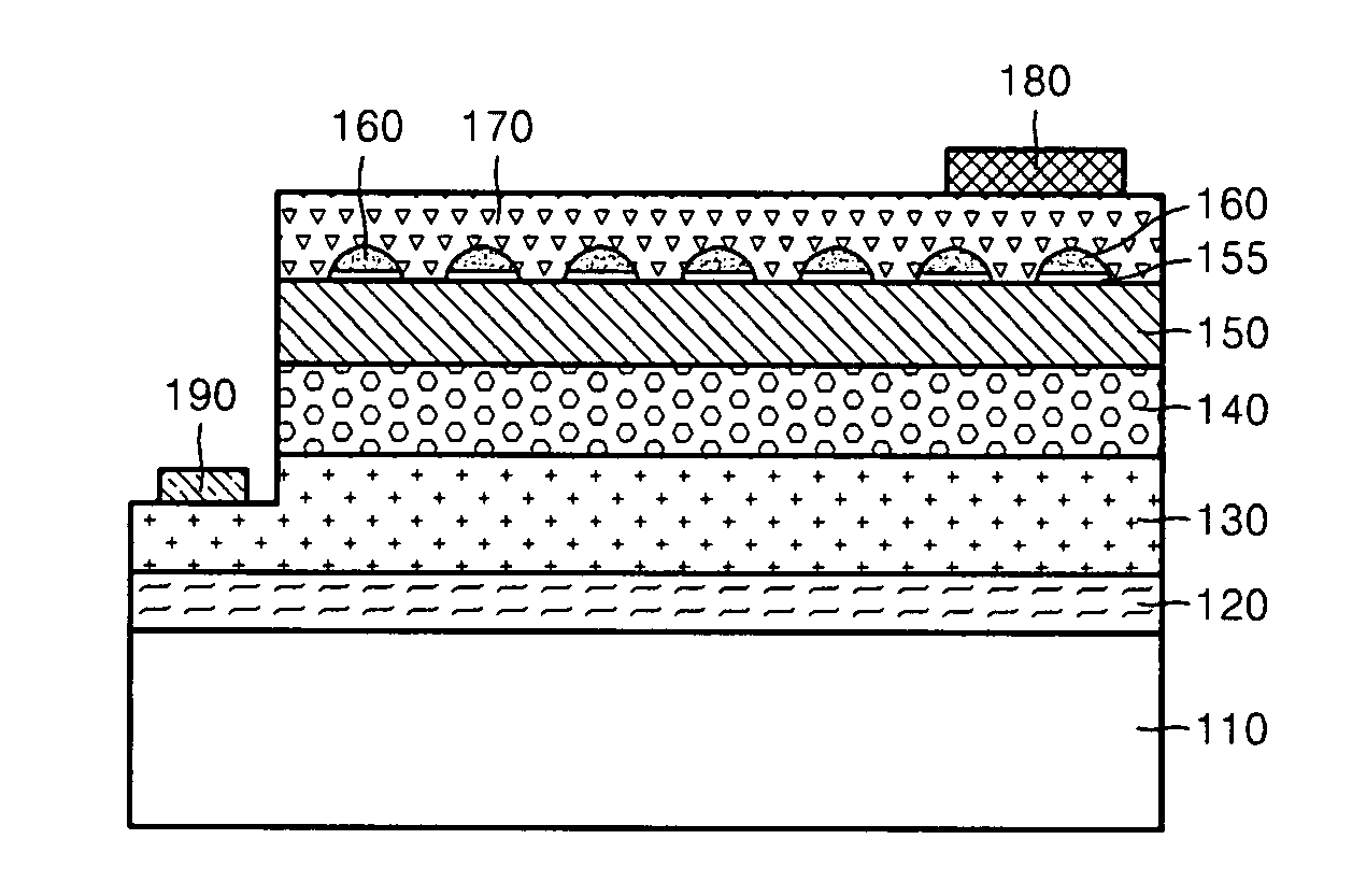
[0039]Referring to FIG. 1, a nitride-based light-emitting device according to the present invention includes a substrate 110, and a buffer layer 120, an n-cladding layer 130, an active layer 140, a p-cladding layer 150, a grid cell layer 160 and a transparent ohmic contact layer 170 sequentially formed on the substrate 110. The nitride-based light-emitting device further includes a p-electrode pad 180 and an n-electrode pad 190.

[0040]The nitride-based light-emitting device is mainly divided into a light-emitting structure including the substrate 110, the buffer layer 120, the n-cladding layer 130, the active layer 140, and the p-cladding layer 150 and a p-electrode structure including the grid cell layer 160 and the transparent ohmic contact layer 170 formed on the p-cladding layer 150. The substrate 110 may be formed from sapphire (Al2O3), silicon carbide (SiC), Si, or gallium arsenide (GaAs). Optionally, the buffer layer 120 may not be formed.

[0041]Each of the layers from the buff...

second embodiment

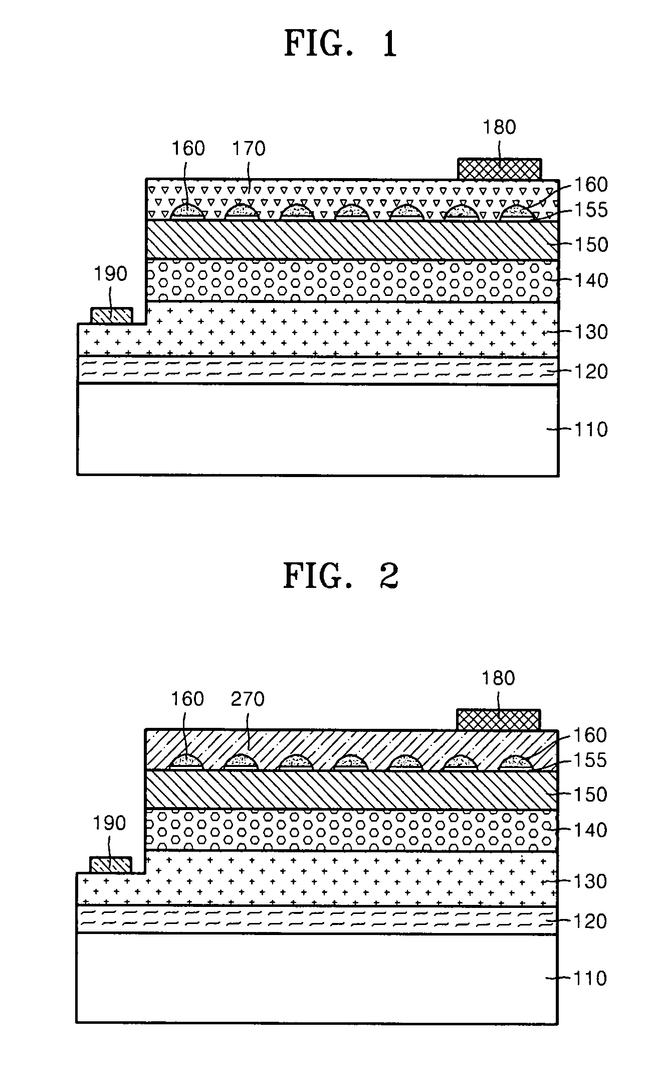
[0053]FIG. 2 is a cross-sectional view of a nitride-based light-emitting device according to the present invention. Referring to FIG. 2, a reflective ohmic contact layer 270 is used as an ohmic contact layer to form a flip-chip structure. Like reference numerals in the drawings denote like elements.

[0054]The reflective ohmic contact layer 270 may be formed in a single layer or multilayers using Au, Ru, Cr, Rh, Sc, Zn, Mg, Ag, Al, or an alloy or solid solution containing at least one selected among the above metals. The reflective ohmic contact layer 270 may also be formed to a thickness of 10 to 1,000 nm.

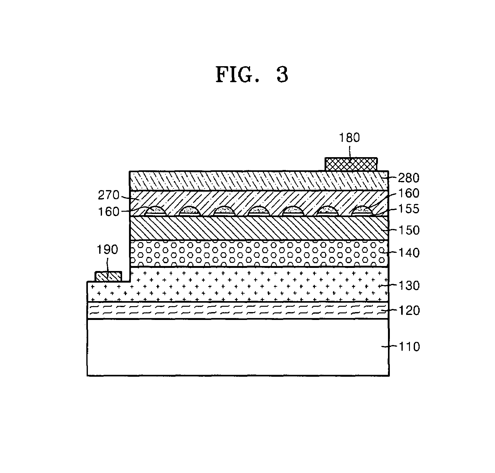
[0055]FIG. 3 is a cross-sectional view of a nitride-based light-emitting device according to a third embodiment of the present invention. Referring to FIG. 3, the nitride-based light-emitting device according to the third embodiment of the present invention further inicudes an agglomeration preventing layer (APL) 280 that is formed on the reflective ohmic contact layer 270 and preve...


PUM


Abstract

A nitride-based light-emitting device and a method of manufacturing the same. The light-emitting device includes a substrate, and an n-cladding layer, an active layer, a p-cladding layer, a grid cell layer and an ohmic contact layer sequentially formed on the substrate. The grid cell layer has separated, conducting particle type cells with a size of less than 30 micrometers buried in the ohmic contact layer. The nitride-based light-emitting device and the method of manufacturing the same improve the characteristics of ohmic contact on the p-cladding layer, thereby increasing luminous efficiency and life span of the device while simplifying a manufacturing process by omitting an activation process after wafer growth.

Description

CROSS-REFERENCE TO RELATED PATENT APPLICATION[0001]This application claims the priority of Korean Patent Application No. 10-2004-0017072, filed on Mar. 12, 2004, in the Korean Intellectual Property Office, the disclosure of which is incorporated herein in its entirety by reference.BACKGROUND OF THE INVENTION[0002]1. Field of the Invention[0003]Embodiments of the present invention relate to a nitride-based light-emitting device and a method of manufacturing the same, and more particularly, to a nitride-based light-emitting device with an electrode structure designed to improve luminous efficiency and a method of manufacturing the same.[0004]2. Description of the Related Art[0005]An ohmic contact between n- and p-electrodes is of great importance in realizing a light-emitting device such as a light-emitting diode (LED) or laser diode (LD) using a gallium nitride (GaN) semiconductor. In particular, an ohmic contact structure between a p-cladding layer and an electrode is essential to t...

Claims


Application Information

Patent Timeline
Patent Type & Authority Patents(United States)
IPC IPC(8): H01L27/15H01L31/12H01L33/00H01L21/28H01L29/22H01L33/06H01L33/32H01L33/38H01L33/42H01S5/323
CPCH01L33/40H01S5/32341H01L33/32H01L33/42H01L2933/0016H01S5/3211
Inventor SEONG, TAE-YEONGKIM, KYOUNG-KOOKSONG, JUNE-OLEEM, DONG-SEOK
Owner SAMSUNG ELECTRONICS CO LTD
Why Eureka
Try Eureka