Film formation method and apparatus for semiconductor process

a film formation method and film technology, applied in the field of film formation methods and apparatus for semiconductor processes, can solve the problems of unsuitable thermal cvd process at high temperature, lower film thickness control, and conventional film formation method cannot meet this requirement, so as to achieve low process temperature, reduce the etching rate of the film, and improve the effect of film thickness control

Inactive Publication Date: 2009-03-24
TOKYO ELECTRON LTD
View PDF4 Cites 69 Cited by
  • Summary
  • Abstract
  • Description
  • Claims
  • Application Information

AI Technical Summary

Benefits of technology

[0014]An object of the present invention is to provide a method and apparatus for forming an insulating film, which can employ a relatively low process temperature in film formation, and cause the etching rate of the film to be lower during a cleaning process, so that the cleaning process can be performed with high controllability in the film thickness, while allowing the film to sufficiently serve as an etching stopper film or inter-level insulating film. It should be noted that the present invention is a modification of the invention disclosed in Jpn. Pat. Appln. KOKAI Publication No. 2003-282566 (Oct. 3, 2003) and US 2006 / 0205231 A1 (Sep. 14, 2006).

Problems solved by technology

However, where a thin film having a low heat resistance is present as an underlayer, a thermal CVD process at high temperature is unsuitable.
Accordingly, the insulating film may be excessively etched by cleaning, and thus the cleaning process entails lower controllability in the film thickness.
However, the conventional film formation method cannot satisfy this requirement.

Method used


Image

  • Film formation method and apparatus for semiconductor process
  • Film formation method and apparatus for semiconductor process
  • Film formation method and apparatus for semiconductor process

Examples


first embodiment

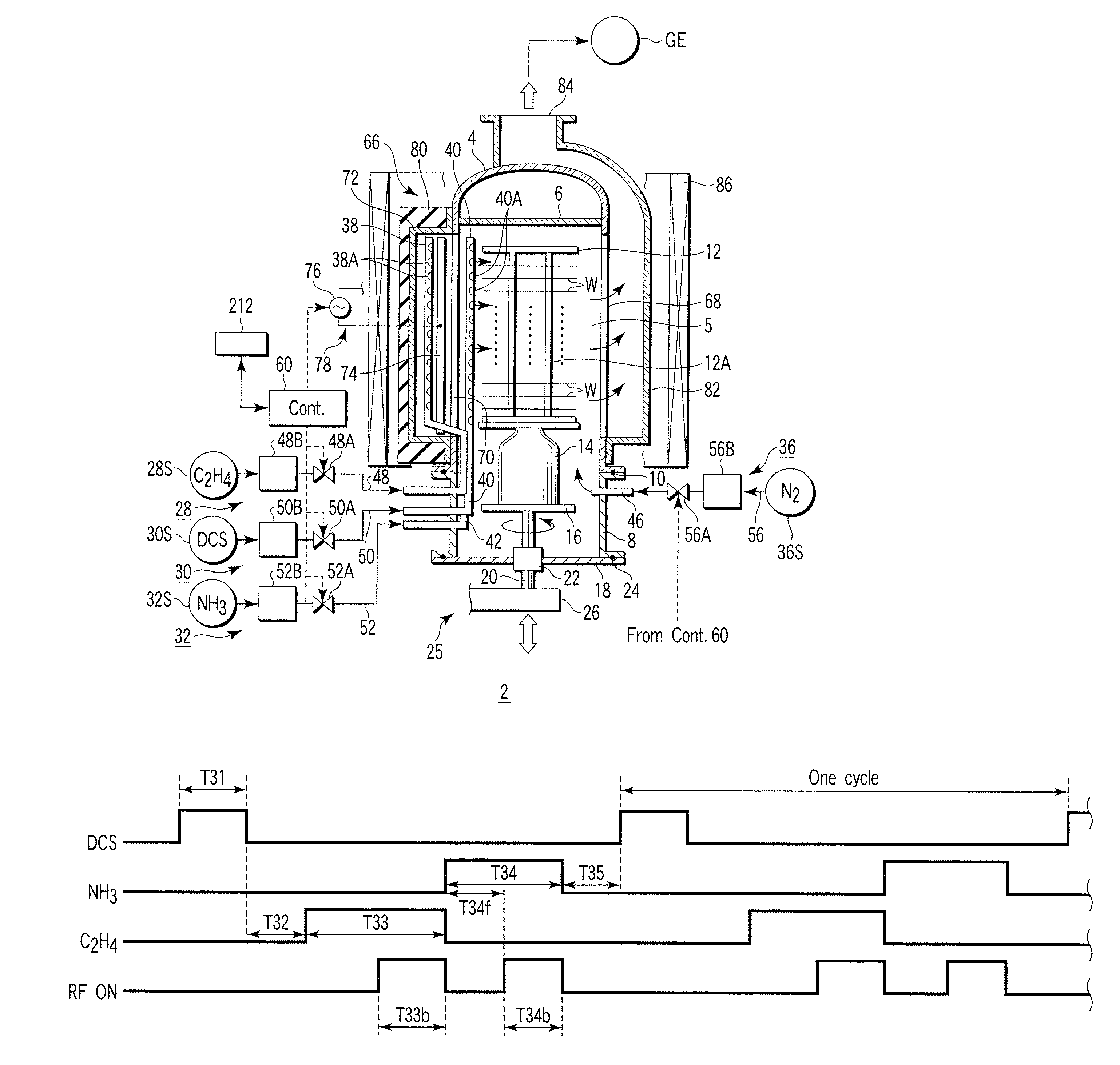
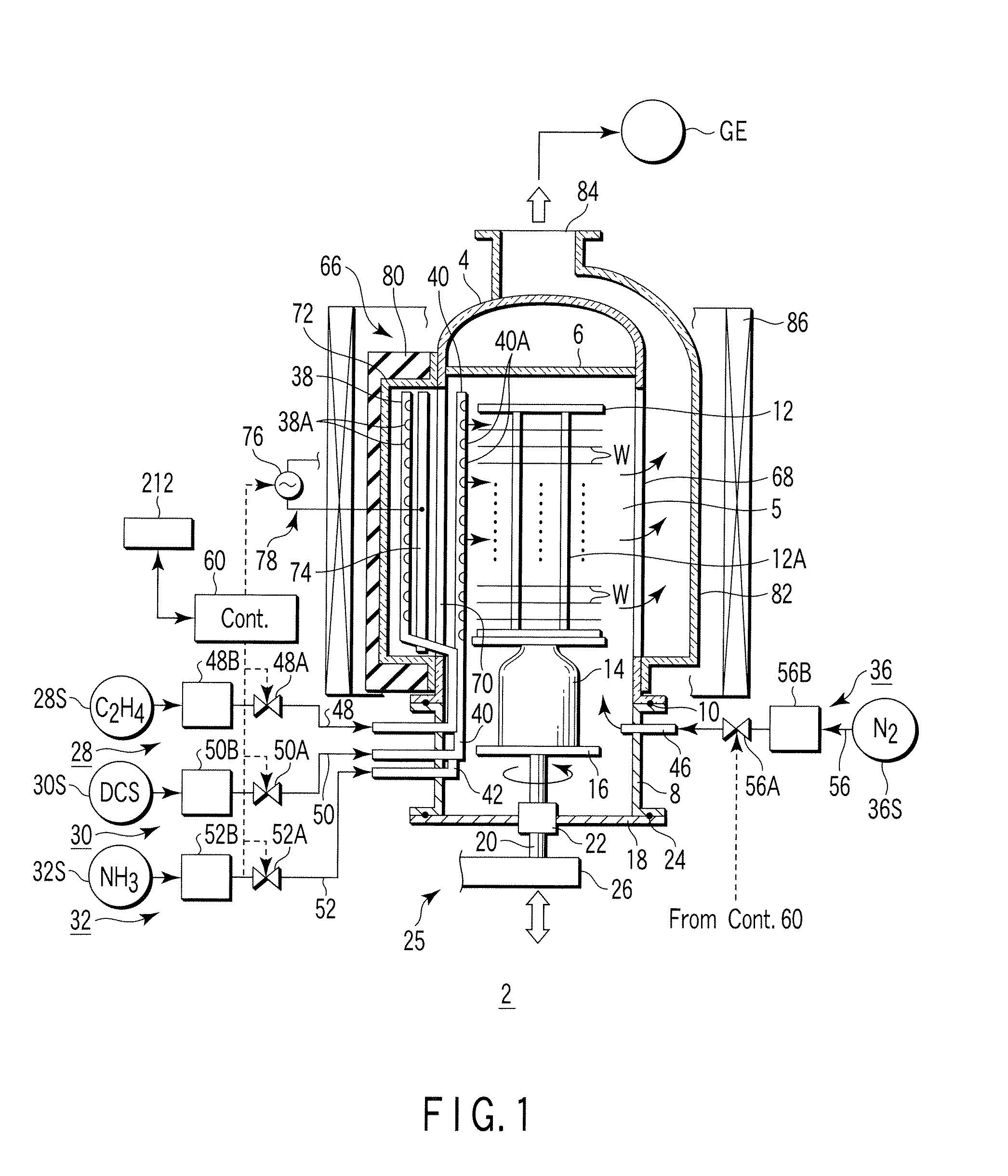
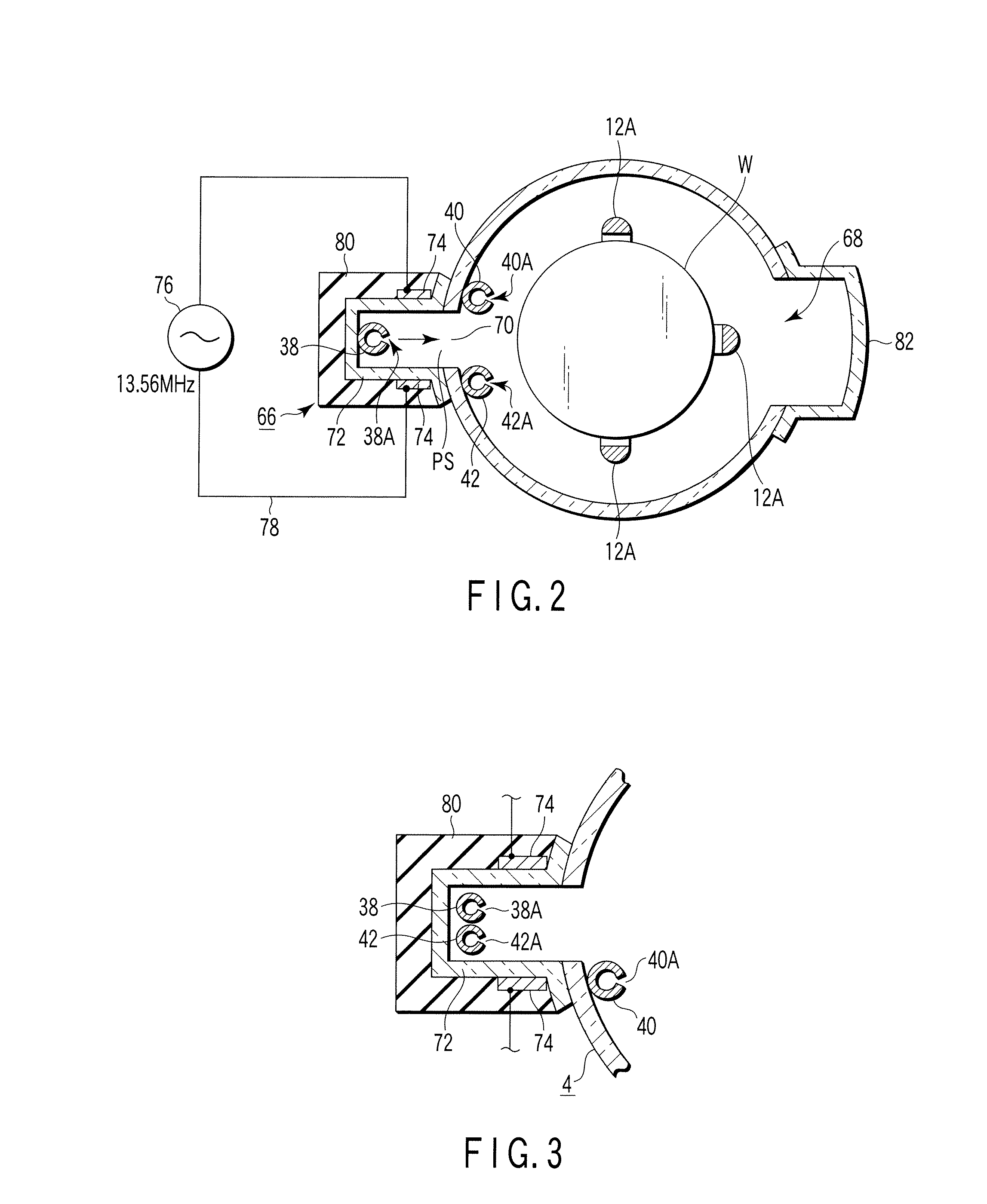
[0107]In the film formation method according to a first embodiment, an insulating film of SiCN (silicon carbon nitride) is formed on semiconductor wafers by CVD. In order to achieve this, a first process gas containing dichlorosilane (DCS) gas as a silane family gas, a second process gas containing ammonia (NH3) gas as a nitriding gas, and a third process gas containing C2H4 gas (ethylene gas) as a carbon hydride gas are selectively supplied into the process field 5 accommodating wafers W.

[0108]At first, the wafer boat 12 at room temperature, which supports a number of, e.g., 50 to 100, wafers having a diameter of 300 mm, is loaded into the process container 4 heated at a predetermined temperature, and the process container 4 is airtightly closed. Then, the interior of the process container 4 is vacuum-exhausted and kept at a predetermined process pressure, and the wafer temperature is increased to a process temperature for film formation. At this time, the apparatus is in a waiting...

second embodiment

[0135]FIG. 8 is a timing chart of the gas supply and RF (radio frequency) application of a film formation method according to the second embodiment of the present invention. As shown in FIG. 8, the film formation method according to this embodiment is arranged to alternately repeat first to fourth steps T11 to T14. A cycle comprising the first to fourth steps T11 to T14 is repeated a number of times, and thin films (unit layers) of SiCN formed by respective cycles are laminated, thereby arriving at an SiCN film having a target thickness.

[0136]Specifically, the first step T11 is arranged to perform supply of the first process gas (denoted as DCS in FIG. 8) and the second process gas (denoted as NH3 in FIG. 8) to the process field 5, while stopping supply of the third process gas (denoted as C2H4 in FIG. 8) to the process field 5. The second step T12 is arranged to stop supply of the first, second, and third process gases to the process field 5. The third step T13 is arranged to perfo...

third embodiment

[0142]FIG. 10 is a timing chart of the gas supply and RF (radio frequency) application of a film formation method according to the third embodiment of the present invention. As shown in FIG. 10, the film formation method according to this embodiment is arranged to alternately repeat first to fourth steps T21 to T24. A cycle comprising the first to fourth steps T21 to T24 is repeated a number of times, and thin films (unit layers) of SiCN formed by respective cycles are laminated, thereby arriving at an SiCN film having a target thickness.

[0143]Specifically, the first step T21 is arranged to perform supply of the first process gas (denoted as DCS in FIG. 10) to the process field 5, while stopping supply of the second process gas (denoted as NH3 in FIG. 10) and the third process gas (denoted as C2H4 in FIG. 10) to the process field 5. The second step T22 is arranged to stop supply of the first, second, and third process gases to the process field 5. The third step T23 is arranged to p...


PUM

PropertyMeasurementUnit
diameteraaaaaaaaaa
frequencyaaaaaaaaaa
frequencyaaaaaaaaaa

Abstract

An insulating film is formed on a target substrate by CVD, in a process field to be selectively supplied with a first process gas containing a silane family gas, a second process gas containing a nitriding gas, and a third process gas containing a carbon hydride gas. This method includes repeatedly performing supply of the first process gas to the process field, supply of the second process gas to the process field, and supply of the third process gas to the process field. The supply of the third process gas includes an excitation period of supplying the third process gas to the process field while exciting the third process gas by an exciting mechanism.

Description

CROSS-REFERENCE TO RELATED APPLICATIONS[0001]This application is based upon and claims the benefit of priority from prior Japanese Patent Application No. 2006-007951, filed Jan. 16, 2006, the entire contents of which are incorporated herein by reference.BACKGROUND OF THE INVENTION[0002]1. Field of the Invention[0003]The present invention relates to a film formation method and apparatus for a semiconductor process for forming an insulating film on a target substrate, such as a semiconductor wafer. The term “semiconductor process” used herein includes various kinds of processes which are performed to manufacture a semiconductor device or a structure having wiring layers, electrodes, and the like to be connected to a semiconductor device, on a target substrate, such as a semiconductor wafer or a glass substrate used for an FPD (Flat Panel Display), e.g., an LCD (Liquid Crystal Display), by forming semiconductor layers, insulating layers, and conductive layers in predetermined patterns ...

Claims


Application Information

Patent Timeline
Patent Type & Authority Patents(United States)
IPC IPC(8): H01L21/31H01L21/469
CPCC23C16/36C23C16/452C23C16/45531C23C16/45546H01L21/3148H01L21/318H01L21/0228H01L21/02211H01L21/02167H01L21/02219
Inventor CHOU, PAO-HWAHASEBE, KAZUHIDE
Owner TOKYO ELECTRON LTD
Why Eureka
Try Eureka