Electrolytic processing apparatus and electrolytic processing method

a processing apparatus and electrolysis technology, applied in the direction of machining working media supply/regeneration, manufacturing tools, lapping machines, etc., can solve the problems of large number of defects that may be produced to deteriorate the properties of workpieces, inability to avoid contamination of workpieces with electrolyte, and denaturation of the resulting film, so as to increase the efficiency of water dissociation and efficiently perform electrolytic processing

Inactive Publication Date: 2009-05-05
EBARA CORP
View PDF27 Cites 2 Cited by
  • Summary
  • Abstract
  • Description
  • Claims
  • Application Information

AI Technical Summary

Benefits of technology

[0020]The present invention has been made in view of the above situation in the related art. It is therefore a first object of the present invention to provide an electrolytic processing apparatus and an electrolytic processing method which can increase the efficiency of the dissociation reaction of water and efficiently perform electrolytic processing, and which can eliminate the need for an operation of a change of ion exchanger.
[0021]It is a second object of the present invention to provide an electrolytic processing apparatus and an electrolytic processing method which can process a surface of a workpiece to greater flatness while minimizing contamination of the surface of the workpiece as well as defects in the surface.

Problems solved by technology

Under these circumstances, in such a conventional machining method that a desired portion in a workpiece is physically destroyed and removed from the surface thereof by a tool, a large number of defects may be produced to deteriorate the properties of the workpiece.
Since an electrolytic solution containing such an electrolyte must be used, contamination of a workpiece with the electrolyte cannot be avoided.
According to this method, the mechanical processing is carried out to the growing surface of a plated film, causing the problem of denaturing of the resulting film.
Chemical mechanical polishing (CMP), for example, generally necessitates a complicated operation and control, and needs a considerably long processing time.
This also imposes a considerable load on the slurry or cleaning liquid waste disposal.
Also in this connection, it is to be pointed out that though a low-k material, which has a low dielectric constant, is expected to be predominantly used in the future as a material for the insulating film (interlevel dielectric layer), the low-k material has a low mechanical strength and therefore it is difficult for it to endure the stress applied during CMP processing.
When an ion exchanger having poor water permeability is used, for example, the supply of water to between a workpiece and an electrode (processing electrode or feeding electrode) is restricted.
The supply of water to the ion exchanger may therefore be insufficient, resulting in a low water decomposition efficiency and thus an insufficient supply of OH− ions or H+ ions as reaction species.
Further, the efficiency of removal of processing products and gasses generated at the surfaces of the workpiece and the electrode during processing will be low.
This may result in deterioration of the morphology of the processed surface.
This method, however, is not a permanent solution yet.
During the change of the ion exchanger, the apparatus must be stopped, leading to a lowering of the throughput.
In electrolytic processing using an electrolyte solution to remove an unnecessary portion of a conductive film having surface irregularities, for example, the copper film 6 embedded in trenches shown in FIG. 1B, formed on a substrate such as a semiconductor wafer, difficulty in flattening the surface irregularities of the conductive film is a typical problem involved in such processing.
This difficulty is ascribable to the fact that an appropriate difference in processing rate between recessed portions and raised portions of the surface irregularities of a conductive film formed on a substrate cannot be produced due to (1) the distance between the substrate and an electrode being much larger than the surface level difference of the conductive film formed on the substrate and (2) low electric resistivity of electrolyte solution.
The sliding movement between the ion exchanger and the workpiece can produce defects in the surface of the workpiece and wear the ion exchanger.

Method used


Image

  • Electrolytic processing apparatus and electrolytic processing method
  • Electrolytic processing apparatus and electrolytic processing method
  • Electrolytic processing apparatus and electrolytic processing method

Examples


Embodiment Construction

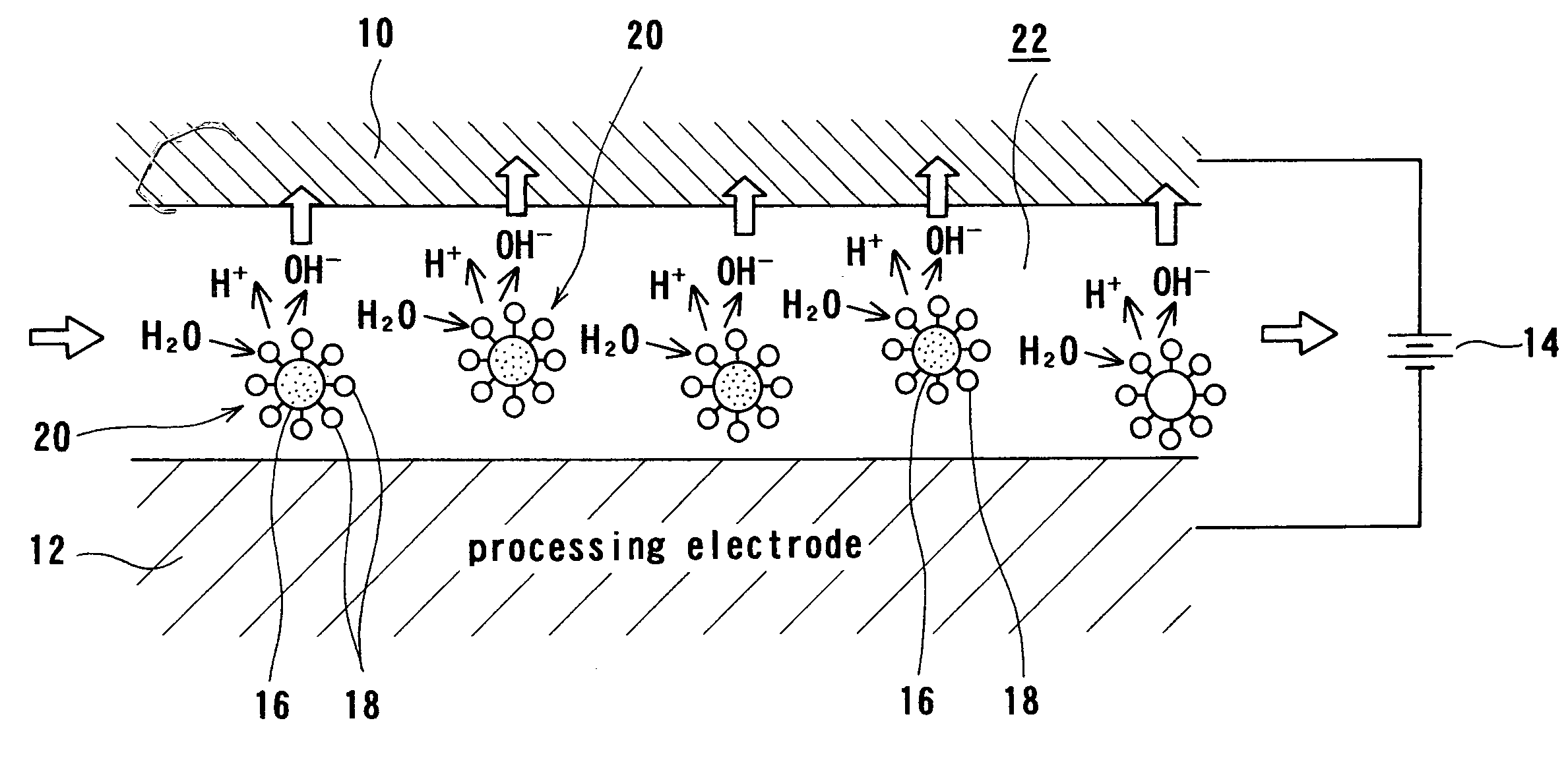
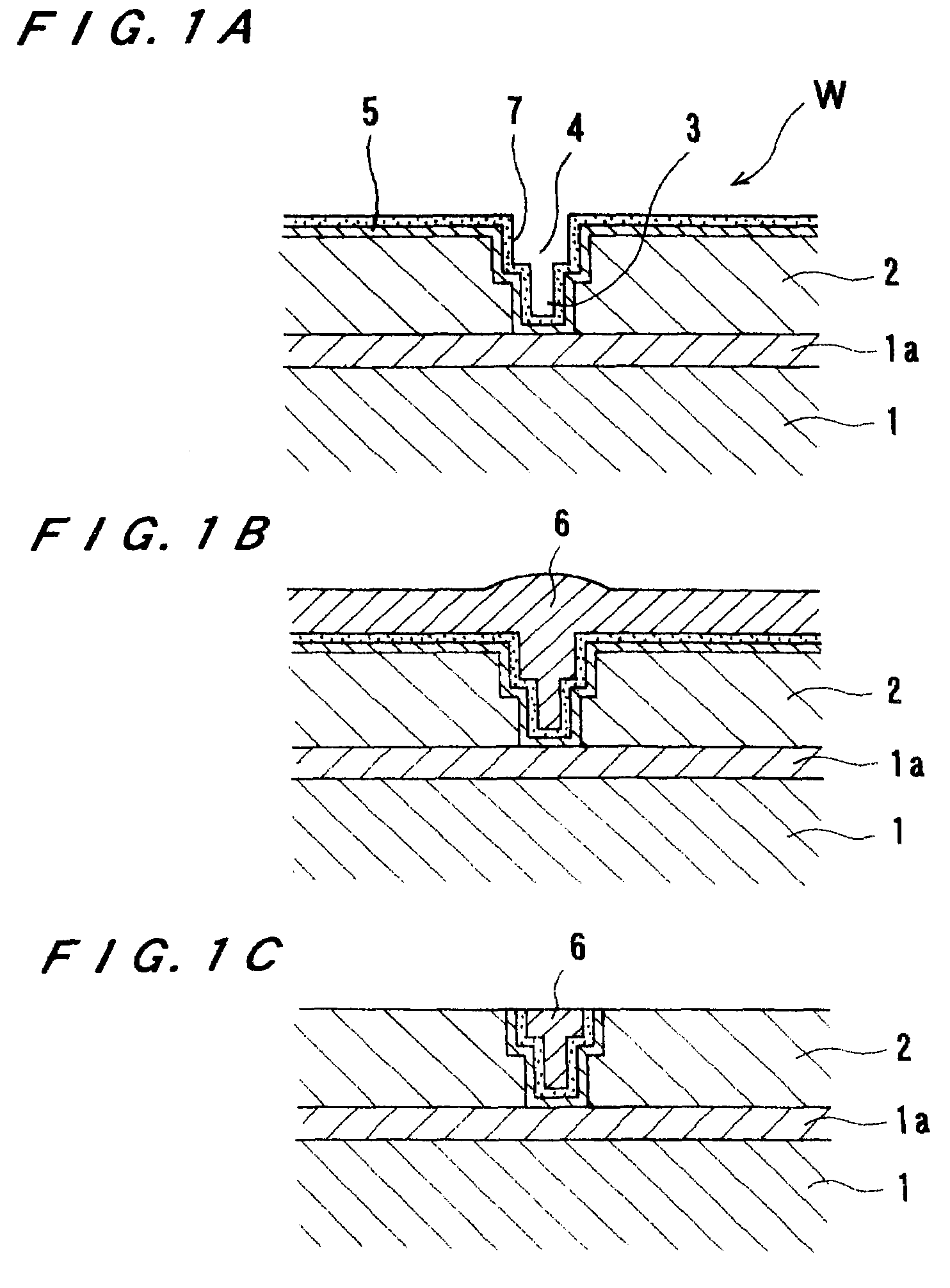
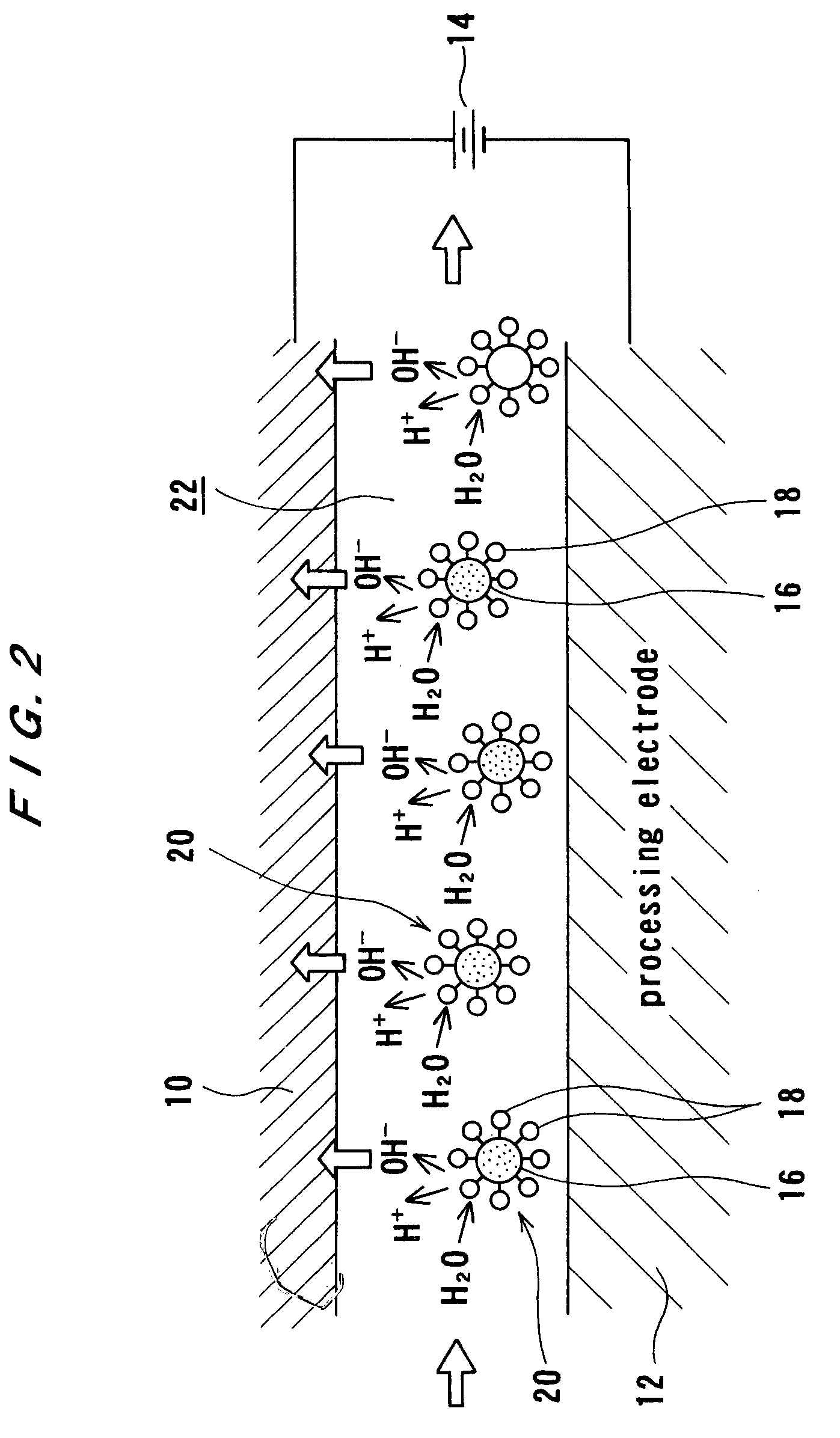
[0088]Preferred embodiments of the present invention will now be described in detail with reference to the drawings. Though the following description illustrates the case of removing a thin film (conductive film), such as a copper film, formed on a surface of a substrate as a workpiece, the present invention is of course applicable to workpieces other than a substrate.

[0089]FIG. 3 is a plan view illustrating the construction of a substrate processing apparatus incorporating an electrolytic processing apparatus according to an embodiment of the present invention. As shown in FIG. 3, the substrate processing apparatus comprises a pair of loading / unloading section 30 as a carry-in / carry-out section for carrying in and out a substrate, e.g. a substrate W having a copper film 6 and a barrier layer as a conductive film (portion to be processed) thereon, as shown in FIG. 1B, a first cleaning machine 31a for performing a primary cleaning of the substrate, a second cleaning machine 31b for p...


PUM

PropertyMeasurementUnit
distanceaaaaaaaaaa
electric conductivityaaaaaaaaaa
thicknessaaaaaaaaaa

Abstract

An electrolytic processing apparatus can increase the efficiency of the dissociation reaction of water and efficiently perform electrolytic processing, and can eliminate the need for an operation of a change of ion exchanger. The electrolytic processing apparatus includes: a processing electrode and a feeding electrode; a liquid supply section for supplying a liquid containing an ion-exchange material between the workpiece and at least one of the processing electrode and the feeding electrode; a power source for applying a voltage between the processing electrode and the feeding electrode; and a drive section for moving the workpiece and at least one of the processing electrode and the feeding electrode relative to each other; wherein electrolytic processing of the workpiece is carried out while keeping the workpiece not in contact with but close to the processing electrode at a distance of not more than 10 μm.

Description

BACKGROUND OF THE INVENTION[0001]1. Field of the Invention[0002]The present invention relates to an electrolytic processing apparatus and an electrolytic processing method, and more particularly to an electrolytic processing apparatus and an electrolytic processing method useful for processing a conductive material formed in a surface of a substrate, such as a semiconductor wafer, or for removing impurities adhering to a surface of a substrate.[0003]2. Description of the Related Art[0004]In recent years, instead of using aluminum or aluminum alloys as a material for forming circuits on a substrate such as a semiconductor wafer, there is an eminent movement towards using copper (Cu) which has a low electric resistivity and high electromigration resistance. Copper interconnects are generally formed by filling copper into fine interconnect recesses formed in a surface of a substrate. Various techniques are known for forming such copper interconnects, including chemical vapor deposition...

Claims


Application Information

Patent Timeline
Patent Type & Authority Patents(United States)
IPC IPC(8): B23H7/36B23H1/10B23H3/10B23H5/08B24B37/04C25F1/00C25F3/00H01L21/321H01L21/768
CPCB23H5/08B24B37/042B24B37/046C25F1/00C25F3/00H01L21/32115H01L21/7684
Inventor KOBATA, ITSUKIWADA, YUTAKAHIYAMA, HIROKUNISAITO, TAKAYUKITOMA, YASUSHISUZUKI, TSUKURUKODERA, AKIRA
Owner EBARA CORP
Why Eureka
Try Eureka