
Tin-coated printed circuit boards with low tendency to whisker formation

a printed circuit board and whisker technology, applied in the field of coated articles, can solve the problems of high process cost, high cost of gold coating, and inability to store for longer than 3 to 6 months

Active Publication Date: 2009-06-16
ENTHONE GMBH
View PDF46 Cites 29 Cited by
  • Summary
  • Abstract
  • Description
  • Claims
  • Application Information

AI Technical Summary

Problems solved by technology

Such metallic finishes are designed for a storage time of up to one year, while purely organic finishes (so-called “OSP”), which are obtained by the treatment of the printed circuit board surface with complexing agents for copper, cannot usually be stored for longer than 3 to 6 months, if the solderability is to be maintained.
Coatings with gold are expensive not only on account of the high gold price, but in addition require special processes for the application of the gold layer.
For example, gold cannot be applied chemically in so-called horizontal plants but only in vertical plants, which additionally results in high process costs.
The application of silver is poorly reproducible, and the necessary plants are difficult to adjust.
A disadvantage of tin surfaces can be seen in the fact that these more or less strongly tend to form, in the course of the storage time, so-called “whiskers”, i.e. needle-shaped tin crystals, which can reach several micrometres in length and which can severely impair the function of a printed circuit board.
Such incidents some years ago finally resulted in tin surfaces only finding reluctant acceptance for certain applications such as flexible printed circuit boards, “tape automated bonding” (TAB) processes and “dupon film” (COF) processes, and in certain regions, such as Japan.
It has not so far been possible completely to elucidate the cause of the whisker formation, however the general view is that mechanical stresses which are transmitted through the printed circuit board into the copper and tin layer, or arise in the tin-coated Cu layer, cause the needle formation in the course of a tension-induced crystallization.
Practical tests have however shown that whisker formation could admittedly be reduced, but not reproducibly and not to the desired extent.
However this process brought hardly any improvement, on the one hand since with too little silver deposition no effect whatever could be achieved, and on the other hand with too great a silver layer thickness (beyond as little as ca.
Ultimately, the desired result could not be achieved with this process.

Method used


Image

  • Tin-coated printed circuit boards with low tendency to whisker formation
  • Tin-coated printed circuit boards with low tendency to whisker formation
  • Tin-coated printed circuit boards with low tendency to whisker formation

Examples


embodiments

Example 1

Production of Coated Printed Circuit Boards

[0077]Epoxy resin composite printed circuit boards were cleaned and degreased using a normal commercial cleaner based on sulphuric acid and citric acid (ACL 7001, Ormecon GmbH) in a cleaning bath for 2 minutes at 45° C. The printed circuit boards used had a test design which has been agreed with test institutes and printed circuit board manufacturers and is modelled on real printed circuit board structures. These boards enable the solderability to be measured and assessed. Next, the printed circuit boards were rinsed with tap-water at room temperature and then treated with an H2O2-containing etching solution (Etch 7000, Ormecon GmbH) for 2 minutes at 30° C. After etching, the boards were again rinsed with tap-water at room temperature. After the rinsing, the printed circuit boards were immersed for 45 secs in a warm aqueous solution or dispersion at 40° C., which contained thiourea (30 g / l), sulphuric acid (20 g / l), 200 mg / l silver...

examples 2 to 7

Production of Coated Printed Circuit Boards (Comparison)

[0084]Analogously to Example 1, printed circuit boards were tinned with normal commercial agents in accordance with the respective use instructions. The products ORMECON CSN (Ormecon GmbH, Ammersbek, Example 2), ORMECON CSN FF (Ormecon GmbH, Ammersbek, Example 3), Shipley Tinposit LT 34 (Example 4), Unicron G 2 (Unicron GmbH, Kirchheimbolanden; Example 5), OMIKRON (Cirtech Co., Florida, USA; Example 6) and Stannatech (Atotech Co., Berlin; Example 7) were used.

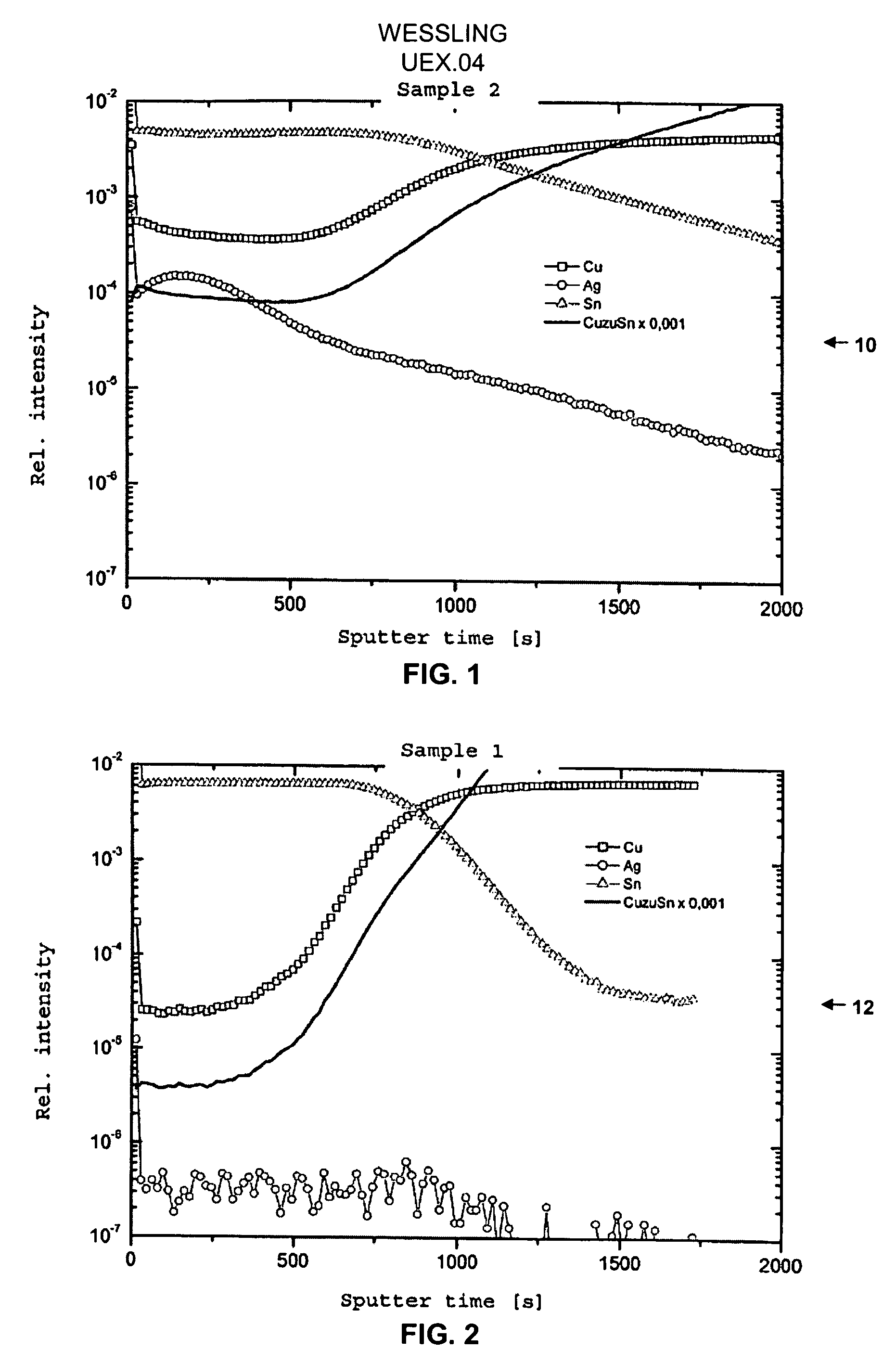
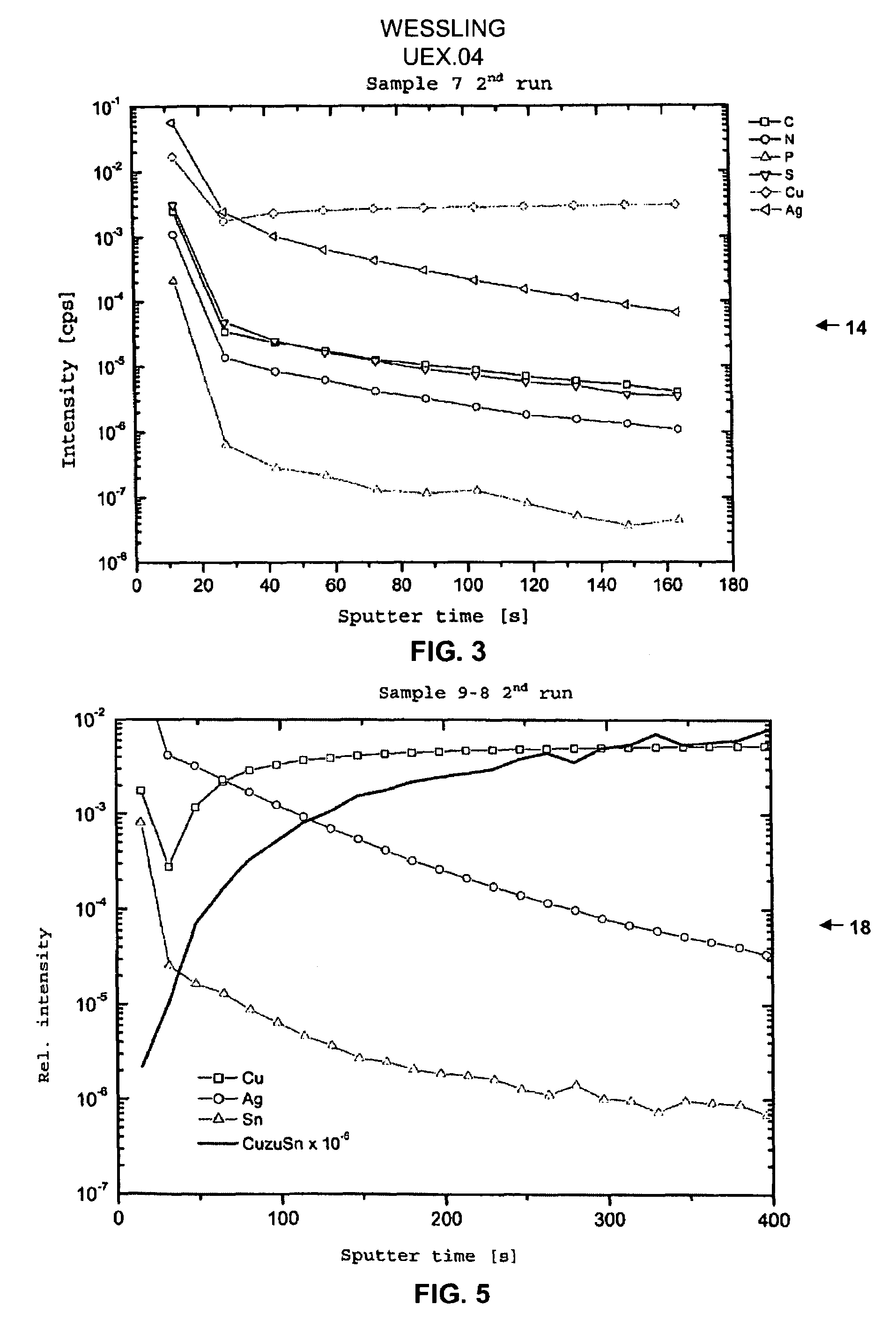
[0085]FIG. 2 shows the secondary ion mass spectrum 12 of the printed circuit board from Comparison Example 3. From a comparison with FIG. 1 it can clearly be seen that the tin and copper concentrations display discontinuous profiles, i.e. the tin layer abruptly decreases at a sputter time of about 900 secs, while the copper concentration abruptly rises at the same time. This indicates a substantial separation of the layers. The copper to tin ratio of 10−4 is already reache...

example 8

Determination of Whisker Size

[0086]The printed circuit boards produced in Examples 1 to 7 were stored for 7 and 14 weeks at room temperature. Next, the plates were examined for the formation of whiskers by optical microscopy and if relevant the size of the whiskers was determined. For this, drill holes of 1 mm diameter were viewed, since whiskers were easier to detect here on account of the dark background. The results are shown below in Table 1.

[0087]

TABLE 1Determination of Whisker SizeStorage Time 7 WksStorage Time 14 WksExampleWhisker SizeWhisker Size1 no whiskersno whiskers2*10-20 μm—1)3*20-30 μm—1)4*>100 μm—1)5*>100 μm—1)6*20-30 μm—1)7*20-30 μm—1)*Comparison Example1)Not Measured

[0088]FIG. 6 shows an optical micrograph 20 of a printed circuit board from Example 1 after storage for 14 weeks. No whisker formation can be discerned.

[0089]FIG. 7 shows an optical micrograph 22 of the printed circuit board from Comparison Example 3 after storage for 7 weeks. The picture is focussed on...


PUM

PropertyMeasurementUnit
sizeaaaaaaaaaa
thicknessaaaaaaaaaa
thicknessaaaaaaaaaa

Abstract

A coated article, which contains (i) at least one electrically non-conductive base layer, (ii) at least one layer of copper and / or a copper alloy, and (iii) a tin-containing layer, wherein the layer (ii) is positioned between the layer (i) and the layer (iii). The article is characterized in that the tin-containing layer (iii) contains at least one other metal.

Description

RELATED APPLICATION DATA[0001]This application claims benefit of commonly assigned and copending German Patent Application Serial Number 10 2004 030 930.2, filed Jun. 25, 2004, entitled TIN-COATED PRINTED CIRCUIT BOARDS WITH LOW TENDENCY TO WHISKER FORMATION, which application is incorporated herein in its entirety by reference.TECHNICAL FIELD[0002]The invention concerns coated articles which contain a layer of copper or a copper alloy and a tin-containing layer, wherein the tin-containing layer contains tin and at least one other metal. The articles are particularly suitable as printed circuit boards or for the production of printed circuit boards.BACKGROUND ART[0003]In general, before their assembly, directly after the production of the conductor track structures, printed circuit boards are provided with a protective layer on the exposed copper surfaces and in the copper-plated drill holes, whose purpose is to guarantee that all soldering points that are to be formed during assemb...

Claims


Application Information

Patent Timeline
Patent Type & Authority Patents(United States)
IPC IPC(8): B32B15/00B32B15/08C23C18/31C23C18/48H05K1/02H05K3/22H05K3/24
CPCC23C18/31C23C18/48H05K3/244H05K2201/0329Y10T428/12861Y10T428/12708Y10T428/12569Y10T428/12514Y10T428/12715H05K2203/072H05K1/09
Inventor WESSLING, BERNHARD
Owner ENTHONE GMBH
Learn More