Multi-phase voltage-control oscillator

a voltage control and oscillator technology, applied in pulse generators, instruments, pulse techniques, etc., can solve the problems of large power consumption of output buffers, large power consumption, and vco noise affecting the noise level of the entire transceiver, and achieve good performan

Inactive Publication Date: 2009-06-23
NAT TAIWAN UNIV OF SCI & TECH
View PDF4 Cites 39 Cited by
  • Summary
  • Abstract
  • Description
  • Claims
  • Application Information

AI Technical Summary

Benefits of technology

[0016]Accordingly, the present invention is directed to providing a multi-phase VCO capable of operating under low voltage and having good performance.
[0018]According to the design concept of the multi-phase VCO of the present invention, the inductors operating indepelectrodeently in the LC tank circuit are cross-coupled to generate an inductance, so as to replace the MOS device originally added to the circuit externally, such that the multi-phase VCO can operates under low supply voltage and has good performance.

Problems solved by technology

As the frequency up- and down-conversion is mainly performed by the mixers at the front electrode of the VCO and the transmitter / receiver, the noise of the VCO will influence the noise level of the entire transceiver.
If the four output buffers are disposed between the filter and the VCO, the output buffer consumes a lot of power.
If the output buffer between the filter and VCO is removed, the capacitance of a resonance cavity increases accordingly, resulting in large power consumption and the increase of the phase noise.
Therefore, the method of generating the quadrature-phase signal has a disadvantage of requiring large chip area.
Therefore, this method has a problem of large power consumption.
However, the method has a disadvantage that the use area is twice of a typical differential VCO area.
However, the oversized coupled MOS device results in that the phase noise get worse due to the extra coupled MOS device, and also incurs an additional current consumption, which leads to a great increase of power consumption.
Although the performance of the second series architecture is better than that of the parallel QVCO, as the stacked MOS devices are disposed in the path from the voltage supply electrode to ground electrode of the series architecture, the circuit cannot operates under low voltage supply.
Therefore, it is a problem to be solved how to operate the multi-phase VCO under low voltage and maintain good performance.

Method used


Image

  • Multi-phase voltage-control oscillator
  • Multi-phase voltage-control oscillator
  • Multi-phase voltage-control oscillator

Examples


first embodiment

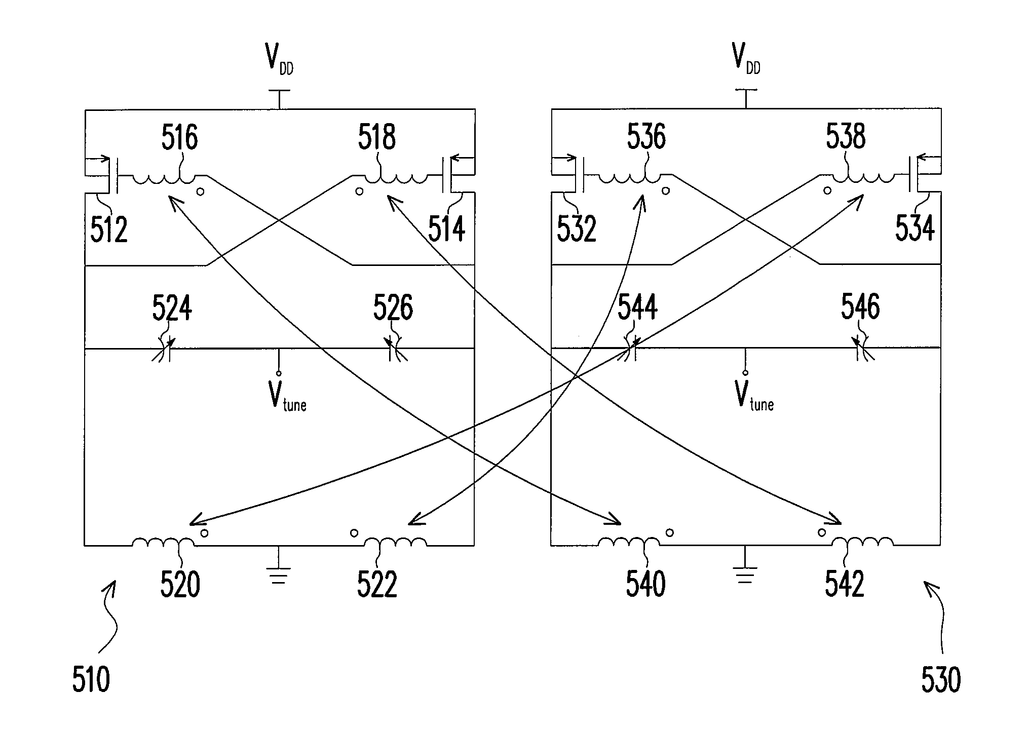
[0033]FIG. 5 is a detailed circuit diagram of a multi-phase VCO according to the present invention. Referring to FIG. 5, the multi-phase VCO provided by this embodiment includes VCO circuits 510 and 530. The VCO circuit 510 includes transistors 512, 514, inductors 516, 518, 520, 522, and varactors 524, 526. Moreover, the VCO circuit 530 includes transistors 532, 534, inductors 536, 538, 540, 542, and varators 544, 546. Since the VCO circuits 510 and 530 are symmetric in the circuit structure, in the following, only the VCO circuit 510 is taken as an example for illustration, and those of ordinary skill in the art can easily deduce the structure of the VCO circuit 530.

[0034]In the VCO circuit 510, the source electrodes of the transistors 512, 514 are coupled with a voltage source VDD, and the drain electrodes are coupled to the respective gate electrodes through the inductors 518 and 516, respectively coupled to a control voltage Vtune through varactors 524, 526, and are grounded thr...

second embodiment

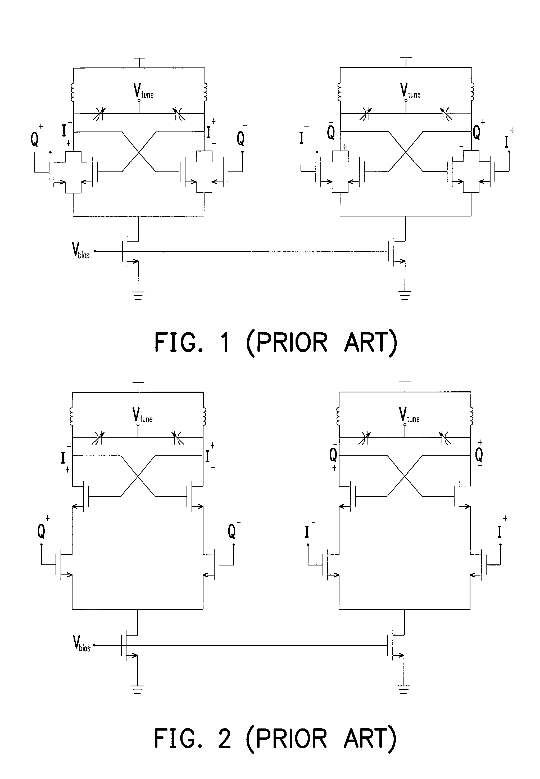
[0037]FIG. 6 is a detailed circuit diagram of a multi-phase VCO according to the present invention. Referring to FIGS. 5 and 6, the multi-phase VCO provided by this embodiment includes VCO circuits 610, 630. The VCO circuit 610 includes transistors 612, 614, inductors 616, 618, 620, 622, and varactors 624, 626. In this embodiment, transistors 612, 614 are, for example, NMOS transistors, and the drain electrodes thereof are respectively coupled to a voltage source VDD through inductors 620, 622, and are respectively coupled to a control voltage Vtune through varactors 624, 626, and the source electrodes are grounded together. In addition, the gate electrodes of the transistors 612, 614 are respectively coupled to the drain electrodes. Further, the back gate electrode of the transistor 612 can be grounded through the inductor 616. Similarly, the back gate electrode of the transistor 614 is grounded through the inductor 618.

[0038]In another aspect, the VCO circuit 630 includes transist...

third embodiment

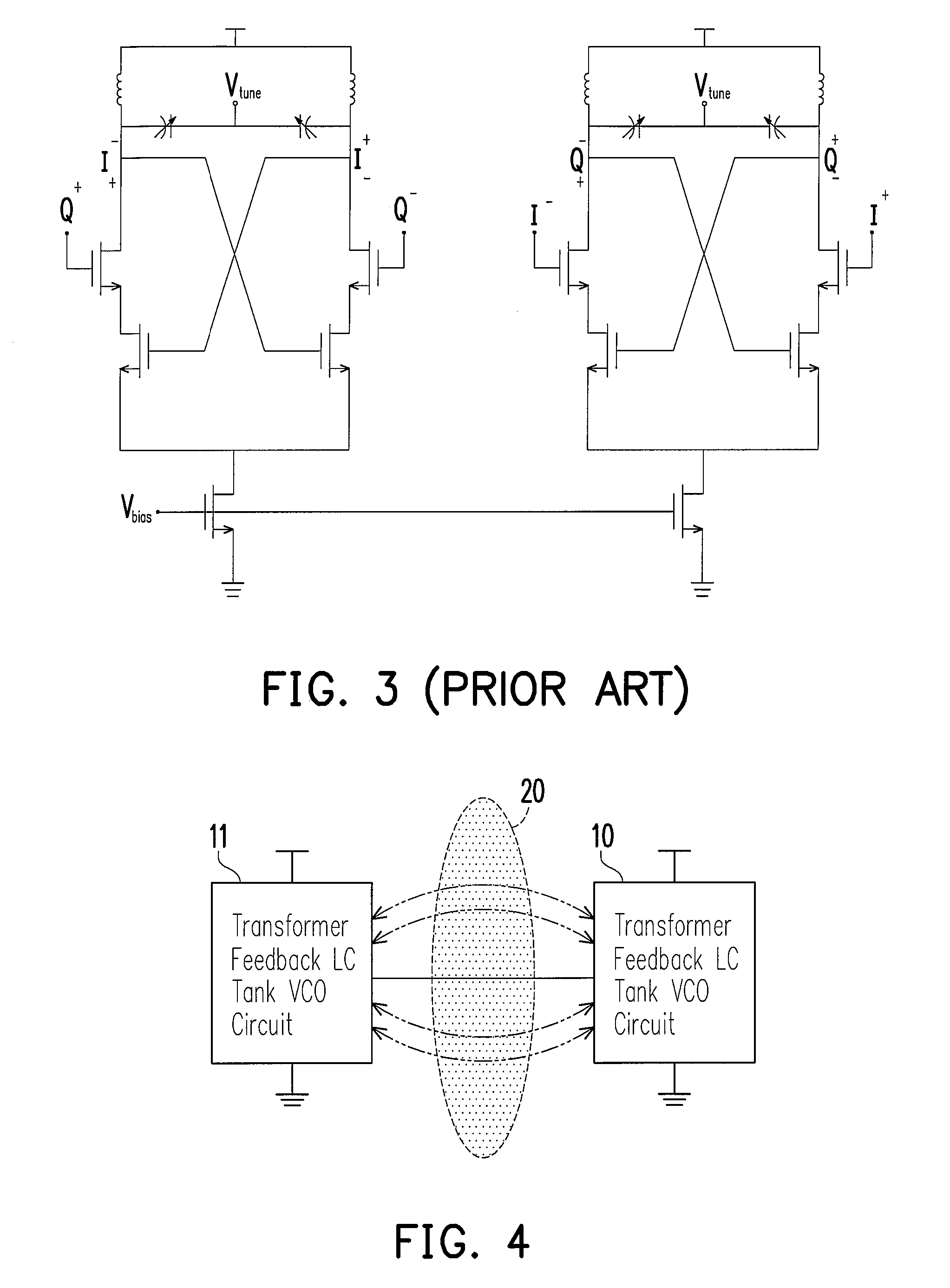
[0039]FIG. 7 is a detailed circuit diagram of a multi-phase VCO according to the present invention. Referring to FIG. 7, the multi-phase VCO provided by this embodiment includes VCO circuits 710 and 730, and the circuit structures of the VCO circuits 710, 730 are substantially the same. Therefore, the VCO circuit 710 is taken as an example for illustration as follows.

[0040]The VCO circuit 710 includes transistors 712 and 714, inductors 716, 718, 720, 722, and varactors 724, 726. The transistors 712 and 714 can be PMOS transistors, the source electrodes thereof are respectively coupled to the voltage source VDD through the inductors 716 and 718, and the drain electrodes are coupled to the respective gate electrodes, coupled to the control voltage Vtune through the varactors 724, 726, and are grounded through the inductors 720, 722.

[0041]Similarly, the VCO circuit 730 also includes transistors 732, 734, inductors 736, 738, 740, 742, and varactors 744, 746, and the coupling manner can ...


PUM


Abstract

A multi-phase voltage-control oscillator including a first voltage-control oscillator circuit and a second voltage-control oscillator circuit is provided. The first voltage-control oscillator circuit includes a first LC tank and a first inductor assembly unit. The second voltage-control oscillator circuit includes a second LC tank and a second inductor assembly unit. A mutual inductance effect is generated between the inductors of the first voltage-control oscillator and the inductors of the second voltage-control oscillator.

Description

CROSS-REFERENCE TO RELATED APPLICATION[0001]This application claims the priority benefit of Taiwan application serial no. 95141131, filed Nov. 7, 2006. All disclosure of the Taiwan application is incorporated herein by reference.BACKGROUND OF THE INVENTION[0002]1. Field of Invention[0003]The present invention relates to a multi-phase voltage-control oscillator (VCO) structure. More particularly, the present invention relates to a structure with inductors between which an inductance effect is generated.[0004]2. Description of Related Art[0005]Currently, with the progress of communication industry, integrated circuits (IC) have been widely applied in wireless communication. In design, the ICs must meet several requirements such as low-voltage operation and low power consumption. In a wireless communication system, after the antenna receives a radio frequency (RF) signal, a frequency down converter constituted of an LNA, a VCO, and a mixer is used to down-convert the RF signal to an in...

Claims


Application Information

Patent Timeline
Patent Type & Authority Patents(United States)
IPC IPC(8): H03B27/00H01L23/66H03B5/12
CPCH03B27/00H03B5/1228H03B5/1296H03B5/1215H03B5/1243H03B2200/0078
Inventor JANG, SHENG-LYANGCHUANG, YUN-HSUEHYEN, REN-HONGLEE, SHAO-HUA
Owner NAT TAIWAN UNIV OF SCI & TECH
Why Eureka
Try Eureka