Method of forming a carbon nanotube-based contact to semiconductor

a technology of carbon nanotubes and contacts, applied in the direction of layered products, transportation and packaging, chemical instruments and processes, etc., can solve the problems of p-gan substrate p-gans with very low conductivity, current injection problems, etc., to achieve low contact resistance interfaces and high optical transmittance of carbon nanotube fabrics

Inactive Publication Date: 2009-07-21
NANTERO
View PDF65 Cites 13 Cited by
  • Summary
  • Abstract
  • Description
  • Claims
  • Application Information

AI Technical Summary

Benefits of technology

[0012]This invention provides a method of forming low contact resistance interfaces between a semiconductor, a fabric of carbon nanotubes and a metal layer, while allowing for a high optical transmittance of the carbon nanotube fabric.
[0029]According to another aspect of the invention, a method of making a conductive article on a semiconductor is provided. The method of making a conductive article on a semiconductor includes providing a semiconductor, forming on the semiconductor a conductive trace including a nonwoven nanotube fabric layer and a thin metal layer, and depositing a mask layer over the conductive trace. The method of making a conductive article on a semiconductor also includes defining a pattern in the mask layer, the pattern corresponding to the shape of the article, and removing portions of the nanotube fabric layer and portions of the metal layer in accordance with the pattern of the mask layer so that the remaining conductive trace forms the conductive article and the semiconductor is substantially preserved.

Problems solved by technology

However, the lack of a stable oxide high manufacturing costs of the III-V semiconductors have prevented them from replacing silicon electronics beyond niche devices and optoelectronic devices (a substantial market itself).
A major challenge in the optoelectronics industry is the ability to form an ohmic, low contact resistance between a metallic (or conductive metal-oxides) thin film and the active p-GaN substrate, which has a very low conductivity.
These thinner metal films may lead to current uniformity and current injection problems into the p-GaN.
Further complicating the development of GaN optical devices are the many issues with processing p-GaN; such as, sensitivity of the active region to photoresists, dry etching and some solvents.
However, neither of these references present or purport to have implemented a process suitable in a manufacturing environment.
More particularly, in both references, the type of nanotubes and the technique employed to deposit the fabric cannot be reproduced in a suitable manufacturing process.
Both the publication by Lee, et. al, and the patent by Rinzler et. al report the use of metal lift-off, which will degrade the device characteristics since the active region is exposed to photoresist, basic developers and solvent chemistries, which damages the active region of the p-GaN, a very sensitive material.

Method used


Image

  • Method of forming a carbon nanotube-based contact to semiconductor
  • Method of forming a carbon nanotube-based contact to semiconductor
  • Method of forming a carbon nanotube-based contact to semiconductor

Examples


example 1

[0083]This device was made using GaN wafers obtained from CREE, Inc., consisting of a p-GaN / n-GaN heterojunction on a SiC substrate and a protective oxide layer. The backside of the wafer was coated with Shipley 1805 photoresist to protect the backside of the wafer during the stripping of the oxide. The wafer was then immersed in a buffered oxide etch to strip the oxide exposing a clean p-GaN surface.

[0084]CNTs were then spun onto the wafer repeatedly until the resistance as measured by a 4-point-probe was about 100Ω. The wafer was then annealed in vacuum at 300° C. for 30 minutes in order to promote adhesion of the CNT fabric and remove residual solvent.

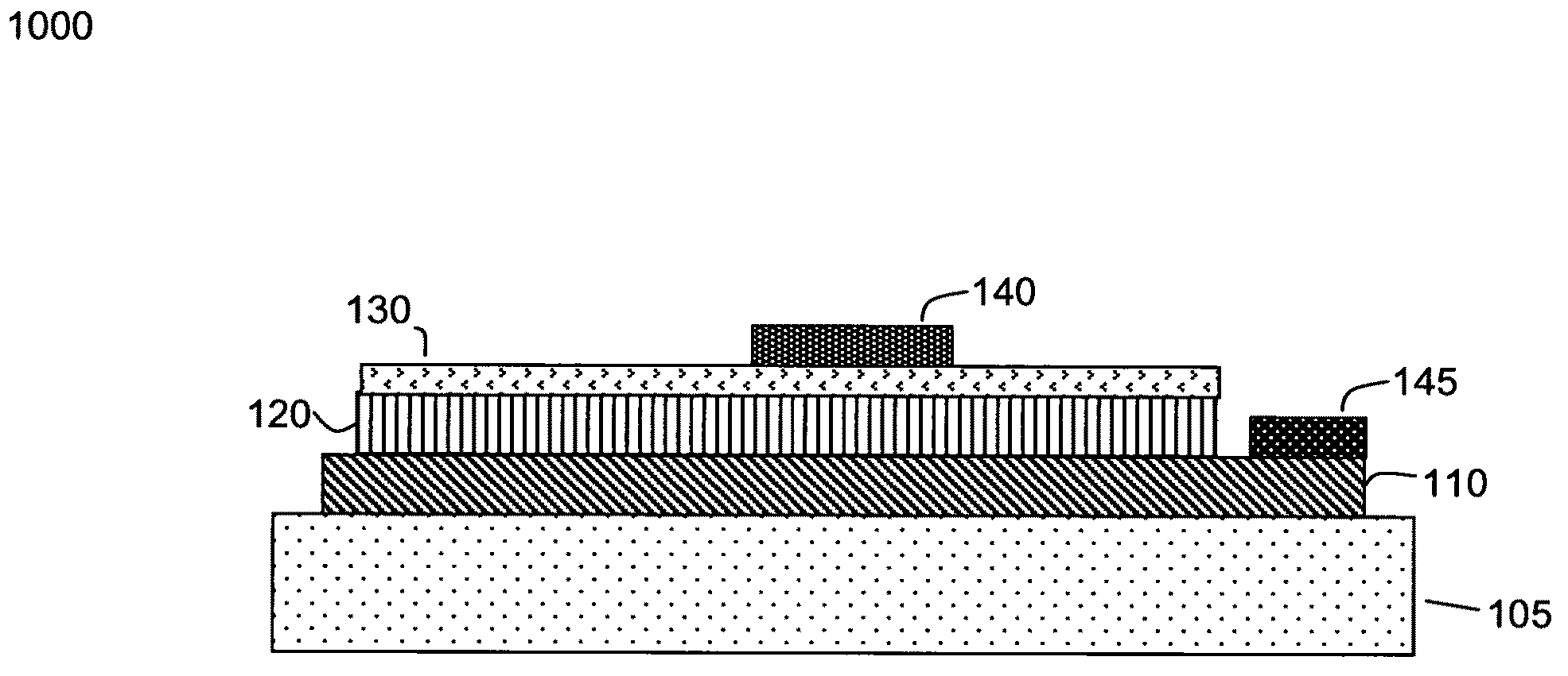
[0085]A metal bi-layer film of 4 nm of Ti and 150 nm of Al were then deposited on top of the CNT fabric by electron beam evaporation. In this case, the CNTs and the 4 nm of Ti comprise the interface layer 350 mentioned in FIG. 3, while the 150 nm of Al comprise the contact pad layer 340.

[0086]Shipley 1805 positive photoresist was th...

example 2

[0094]The following is an example of a process sequence used to form CNT contacts to p-GaN with aluminum contacting the CNT pad. This particular embodiment of the invention should be considered illustrative and not restrictive.

[0095]The substrates used in the experiment described in this example were films p-GaN on sapphire (alumina) substrates which had gold contacts on the bottom side of the wafer and came with a protective sputtered SiO2 layer on the p-GaN layer to protect the film from corrosion, oxidation and damage. The samples were obtained from CREE Inc.

[0096]The following process steps were employed:

(a) Strip pGaN sputtered SiO2 with ammoniumfluoride: A solution called Timetech® (ammonium fluoride) was used at room temperature to dissolve the 200 nm thick protective film of sputtered SiO2.

(b) Deposit CNTs (spray): With the wafer held at 120 C on a hotplate, an aqueous solution of carbon nanotubes was sprayed onto the substrate until the CNT transparency reached about 90% an...


PUM

PropertyMeasurementUnit
mechanical strengthaaaaaaaaaa
diametersaaaaaaaaaa
sheet resistanceaaaaaaaaaa

Abstract

Manufacturers encounter limitations in forming low resistance ohmic electrical contact to semiconductor material P-type Gallium Nitride (p-GaN), commonly used in photonic applications, such that the contact is highly transparent to the light emission of the device. Carbon nanotubes (CNTs) can address this problem due to their combined metallic and semiconducting characteristics in conjunction with the fact that a fabric of CNTs has high optical transparency. The physical structure of the contact scheme is broken down into three components, a) the GaN, b) an interface material and c) the metallic conductor. The role of the interface material is to make suitable contact to both the GaN and the metal so that the GaN, in turn, will make good electrical contact to the metallic conductor that interfaces the device to external circuitry. A method of fabricating contact to GaN using CNTs and metal while maintaining protection of the GaN surface is provided.

Description

CROSS-REFERENCE TO RELATED APPLICATIONS[0001]This application is a continuation-in-part of and claims priority under 35 U.S.C. §120 to U.S. patent application Ser. No. 11 / 111,582, filed on Apr. 21, 2005, entitled NANOTUBE FILMS AND ARTICLES, which is a continuation of U.S. patent application Ser. No. 10 / 776,573, filed on Feb. 11, 2004, now U.S. Pat. No. 6,942,921, which is a continuation of U.S. patent application Ser. No. 10 / 128,118, filed Apr. 23, 2002, now U.S. Pat. No. 6,706,402, and hereby incorporates such references in their entirety.[0002]This application also claims priority under 35 U.S.C. §119(e) to U.S. Provisional Patent Application No. 60 / 775,461, filed on Feb. 21, 2006, entitled METHOD OF FORMING CARBON NANOTUBE-BASED CONTACT TO SEMICONDUCTOR which is incorporated herein by reference in its entirety.[0003]Additionally, this application claims priority under 35 U.S.C. § 120 to U.S. patent application Ser. No. 10 / 341,130, filed on Jan. 13, 2003, entitled CARBON NANOTUBE...

Claims


Application Information

Patent Timeline
Patent Type & Authority Patents(United States)
IPC IPC(8): H01L21/44H01L33/32H01L33/40
CPCB82Y20/00H01L21/28575H01L29/417H01L33/40H01L29/452H01L29/2003Y10T428/30H01L33/32Y10S438/924Y10T428/31678
Inventor WARD, JONATHAN W.SCHLATKA, BENJAMINMEINHOLD, MITCHELLSMITH, ROBERT F.SEGAL, BRENT M.
Owner NANTERO
Why Eureka
Try Eureka