Monolithic high aspect ratio nano-size scanning probe microscope (SPM) tip formed by nanowire growth

a scanning probe and nanowire technology, applied in the field of scanning microscope probes, can solve the problems similar to micro-machined afm tips, and achieve the effects of low cost of manufactured tips, easy growth, and reliability and durability advantages

Inactive Publication Date: 2009-08-11
GLOBALFOUNDRIES INC
View PDF6 Cites 26 Cited by
  • Summary
  • Abstract
  • Description
  • Claims
  • Application Information

AI Technical Summary

Benefits of technology

[0011]The inventive structure and methods described herein provide several advantages over the prior art. First, the fabrication of the tips is a batch process in which all steps are conventional silicon processing steps. As such, many tips can be fabricated in parallel on a single silicon wafer as illustrated by FIG. 2. As a result, the cost of the manufactured tip is expected to be low and similar to that of a micromachined AFM tip. Moreover, the performance delivered by the tip disclosed in the present invention is that of a high aspect ratio nanometer size radius tip that currently cost 1000× more than a conventional micromachined tip.
[0012]Second, the inventive silicon nanowire is grown epitaxially (i.e., from the same crystal structure) from the tip of the micromachined AFM tip. As such, there is a seamless interface between the AFM tip and the nanowire. This gives the inventive tip a reliability and durability advantage over prior art tips where a CNT is glued to the end of the AFM tip.
[0013]Third, nanowires of different materials (e.g., Ge or GaAs) can be easily grown epitaxially on the silicon AFM tip allowing different chemical terminations for the probe, and also different mechanical properties.

Problems solved by technology

As a result, the cost of the manufactured tip is expected to be low and similar to that of a micromachined AFM tip.

Method used


Image

  • Monolithic high aspect ratio nano-size scanning probe microscope (SPM) tip formed by nanowire growth
  • Monolithic high aspect ratio nano-size scanning probe microscope (SPM) tip formed by nanowire growth
  • Monolithic high aspect ratio nano-size scanning probe microscope (SPM) tip formed by nanowire growth

Examples


example

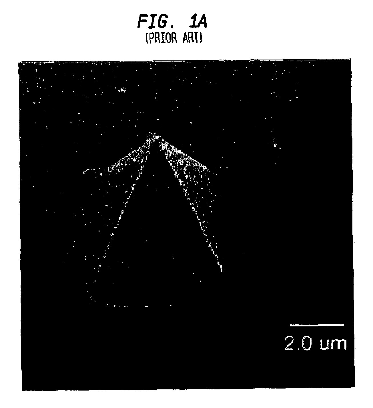
[0049]In this example, a micromachined silicon pyramid extended by a silicon nanowire using the method outlined in FIGS. 3A-3C was provided. Specifically, a silicon wafer was masked and etched in KOH to form silicon pyramids. The native oxide was removed by an HF dip and a 2 nm thick gold film was evaporated over the silicon pyramid. The wafer was then loaded into an UHV-CVD furnace. A pre-growth anneal at 500° C. in H2 ambient for 10 minutes was used to agglomerate the Au film into AuSi eutectic droplets. The furnace temperature was then lowered to the nanowire growth temperature of 420° C. Pure silane (SiH4) at a pressure of 2 torr was used as the precursor. FIGS. 6A-6B are SEM images showing a silicon pyramid following the growth. The typical length of the silicon nanowires is about 700 nm and their typical diameter is about 10-12 nm.

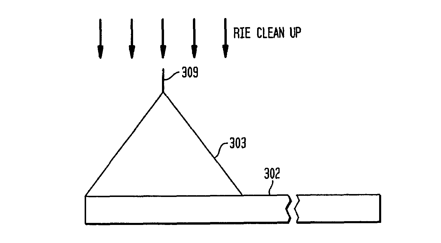
[0050]Following the growth the wafer was etched by RIE using CF4 chemistry. As can be seen in FIGS. 7A-7B the non-vertical nanowires are etched off ...


PUM

PropertyMeasurementUnit
temperatureaaaaaaaaaa
lengthaaaaaaaaaa
temperatureaaaaaaaaaa

Abstract

A scanning probe where the micromachined pyramid tip is extended by the growth of an epitaxial nanowire from the top portion of the tip is disclosed. A metallic particle, such as gold, may terminate the nanowire to realize an apertureless near-field optical microscope probe.

Description

DISCRIPTION[0001]1. Field of the Invention[0002]The present invention relates to scanning microscope probes, and more specifically to a monolithic silicon probe made of an etched silicon pyramid with its tip extended with a Si nanowire. The present invention also relates to methods of fabricating the silicon probe and the nanowire extension.[0003]2. Background of the Invention[0004]Scanning Probe Microscopy (SPM) techniques such as Atomic Force Microscopy (AFM) and Near-Field Scanning Optical Microscopy (NSOM) are very useful techniques for the study of surfaces. Acquired SPM images provide surface properties (e.g., topography or roughness) on a nanometer scale. As a result, SPM instruments are now used routinely for testing in industries where small dimensions are involved. A typical example is the semiconductor industry where AFM is used to evaluate the surface roughness and topography following a film deposition or a chemical mechanical polishing (CMP) step. Another important app...

Claims


Application Information

Patent Timeline
Patent Type & Authority Patents(United States)
IPC IPC(8): G12B21/02G01Q70/12B81C99/00G01Q60/22G01Q60/38G01Q70/16
CPCB82Y15/00B82Y20/00G01Q70/12G01Q60/22B82Y35/00
Inventor COHEN, GUY M.HAMANN, HENDRIK F.
Owner GLOBALFOUNDRIES INC
Why Eureka
Try Eureka