MOS transistor with self-aligned source and drain, and method for making the same

a technology of metal oxidesemiconductor and self-aligning source, which is applied in the direction of basic electric elements, semiconductor devices, electrical equipment, etc., can solve the problems that the combination of known process technologies is not compatible with low-cost electronics, and achieves low cost, reliable, and commercially acceptable electrical characteristics. , the effect of low cos

Inactive Publication Date: 2009-11-17
ENSURGE MICROPOWER ASA
View PDF25 Cites 65 Cited by
  • Summary
  • Abstract
  • Description
  • Claims
  • Application Information

AI Technical Summary

Benefits of technology

[0006]The present invention advantageously provides a low cost method for making MOS thin film transistors (MOS TFTs) having reliable, commercially acceptable electrical characteristics (e.g., on / off speeds, on / off ratios, carrier mobilities, threshold voltages [Vt's], etc.). Printed and / or radiation-defined (e.g., laser-written, as opposed to photolithographically produced) semiconductor structures and (optionally) conductor structures provide results similar to those produced by more conventional semiconductor processing at a much lower cost and at a much higher throughput (on the order of hours to days, as opposed to weeks to months using conventional MOS semiconductor process technology). These and other advantages of the present invention will become readily apparent from the detailed description of preferred embodiments below.

Problems solved by technology

However, this combination of known process technologies is not compatible with low cost electronics, both for overall cost considerations and for low-cost process temperature limitations.

Method used


Image

  • MOS transistor with self-aligned source and drain, and method for making the same
  • MOS transistor with self-aligned source and drain, and method for making the same
  • MOS transistor with self-aligned source and drain, and method for making the same

Examples


second embodiment

[0040]In a second embodiment, a conductor ink may be printed onto dielectric layer 14 by essentially any conventional printing technology. For example, printing may comprise inkjetting, gravure printing, offset printing, flexography (flexo-printing), spray-coating, slit coating, extrusion coating, meniscus coating, microspotting, pen-coating, and / or laser forward transferring the conductor in a predefined pattern onto dielectric layer 14. The ink may comprise or consist essentially of the metal precursor and a solvent. The metal precursors that are generally compatible with printing (or plating onto a printed conductor or semiconductor precursor) may comprise nanoparticles or nanocrystals of a metal such as titanium, copper, silver, chromium, molybdenum, tungsten, cobalt, nickel, gold, palladium, platinum, zinc, iron, etc., or metal alloys thereof, preferably silver or gold (or a metal alloy thereof). Such nanoparticles or nanocrystals may be conventionally passivated (e.g., with on...

first embodiment

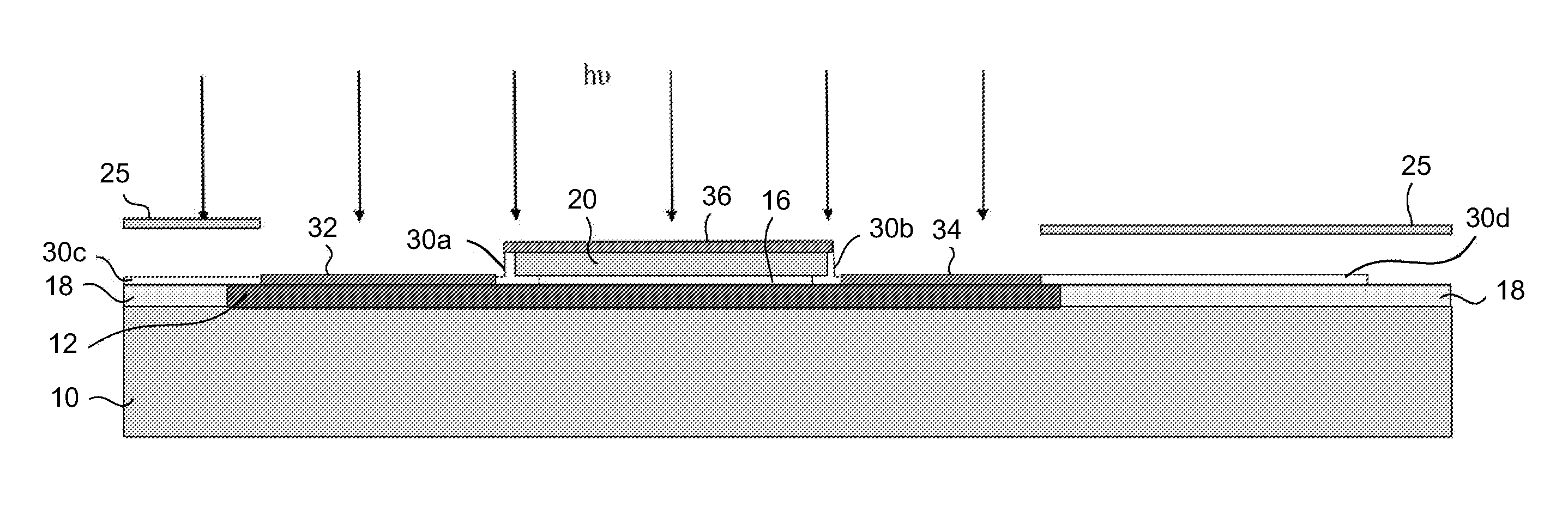
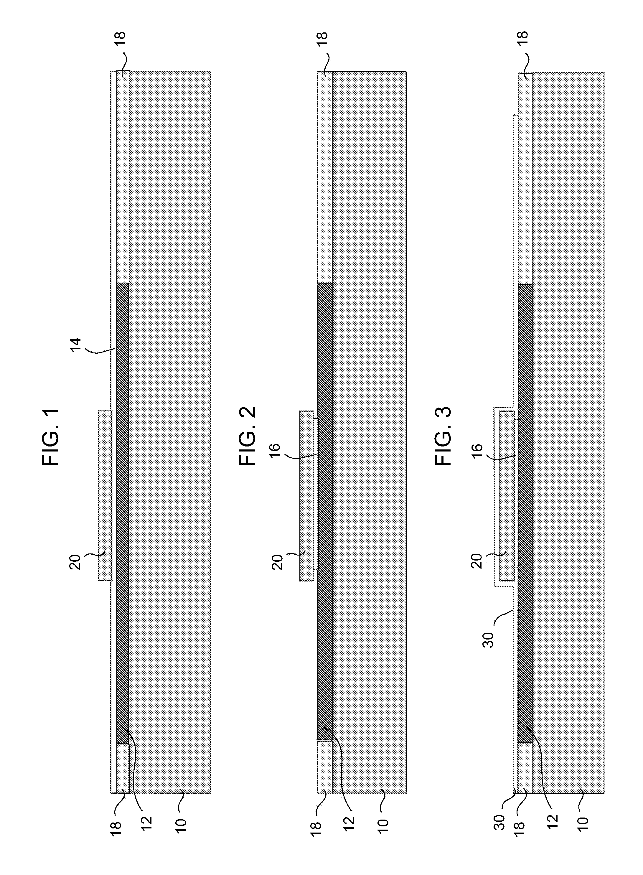
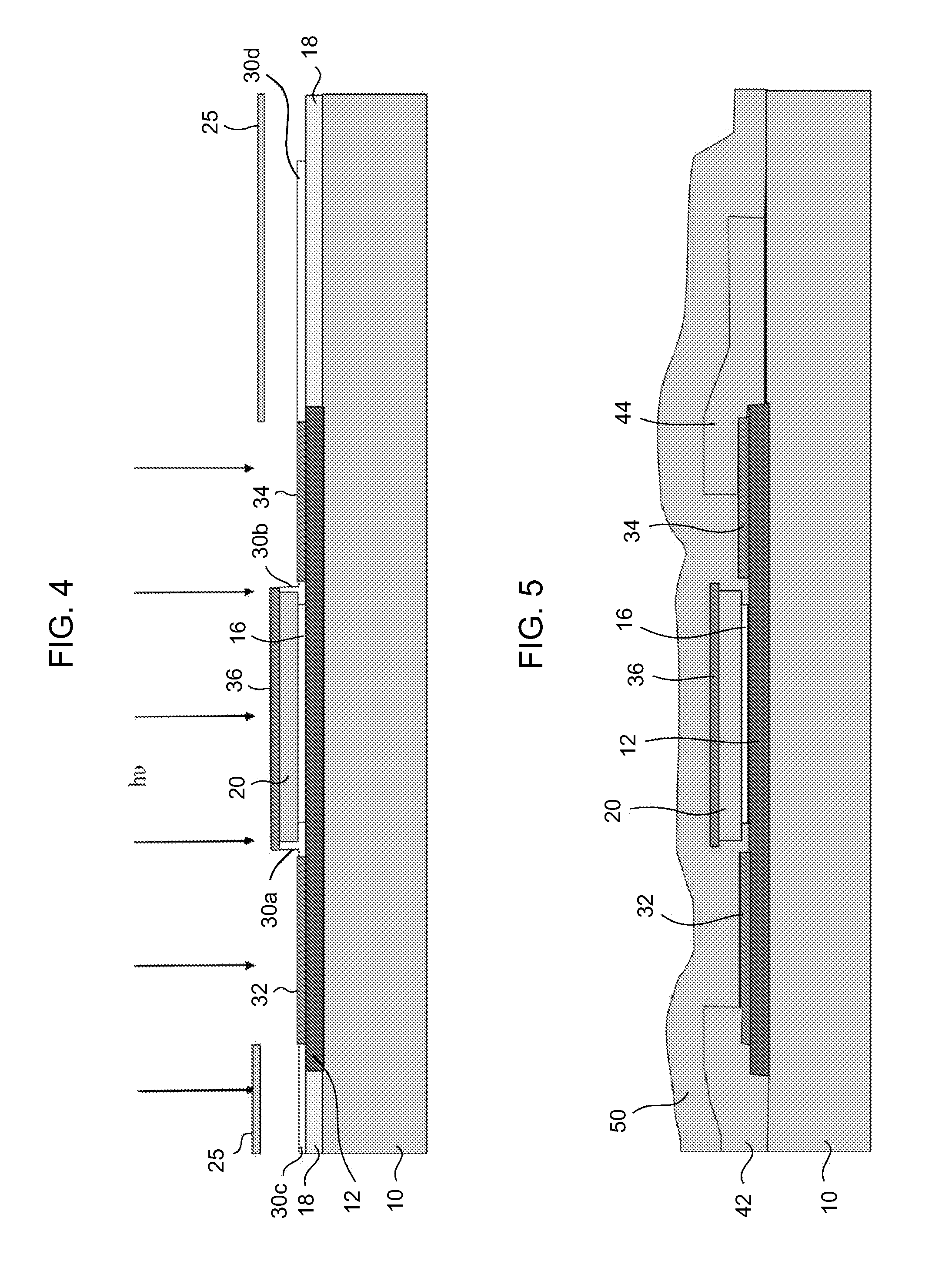
[0045]The present method may further comprise the steps of forming dielectric layer 14 and / or forming electrically functional (preferably, semiconductor) layer 12. In one embodiment, semiconductor layer 12 may be formed by the same techniques as the first embodiment for forming gate metal 20, but using conventional semiconductor (or semiconductor precursor) materials for blanket deposition. As is known in the art, conventional blanket deposition may comprise chemical vapor deposition (CVD), low pressure CVD, sputtering or other physical vapor deposition (PVD) technique, spin coating, spray coating, etc. Preferably, such blanket deposition comprises CVD of a silane (e.g., SiH4) and / or germane (e.g., GeH4). The blanket-deposited semiconductor layer 12 may be lightly doped, e.g., by conventional ion implantation (and optionally, subsequent annealing). Active transistor regions (e.g., an area of semiconductor layer 12 that is substantially defined by the outermost borders of the overlyi...


PUM


Abstract

A MOS transistor with self-aligned source / drain terminals, and methods for its manufacture. The transistor generally includes an electrically functional substrate, a dielectric film on portions of the substrate, a gate on the dielectric film, and polycrystalline source and drain terminals self-aligned with the gate. The method generally includes forming an amorphous semiconductor material on a gate and on exposed portions of an electrically functional substrate, irradiating an upper surface of the amorphous semiconductor material to form self-aligned polycrystalline semiconducting source / drain terminal layers, and (optionally) selectively removing the non-irradiated amorphous semiconductor material portions. The present invention advantageously provides MOS thin film transistors having reliable electrical characteristics quickly, efficiently, and / or at a low cost by eliminating one or more conventional photolithographic steps.

Description

RELATED APPLICATIONS[0001]This application may be related to U.S. Provisional Application No. 60 / 663,296, filed Mar. 18, 2005, entitled “MOS Transistor with Metal Gate, and Method for Making the Same,” which (to the extent possible) is incorporated herein by reference in its entirety.FIELD OF THE INVENTION[0002]The present invention generally relates to the field of metal-oxide-semiconductor (MOS) transistors and methods of making the same. More specifically, embodiments of the present invention pertain to MOS thin film transistor structures having self-aligned source / drain terminals and methods for their manufacturing and / or production using a liquid silane precursor and / or printing techniques.DISCUSSION OF THE BACKGROUND[0003]The feasibility of building a GHz thin film transistor (TFT), as well as technology to measure the characteristics of such TFTs, is known in the art (see, e.g., Wang et al., Hong Kong University of Science and Technology). Metal induced lateral crystallizatio...

Claims


Application Information

Patent Timeline
Patent Type & Authority Patents(United States)
IPC IPC(8): H01L31/00
CPCH01L29/04H01L29/78618H01L29/66757
Inventor CLEEVES, JAMES MONTAGUE
Owner ENSURGE MICROPOWER ASA
Why Eureka
Try Eureka