Method for fabricating capacitor of semiconductor device

a semiconductor device and capacitor technology, applied in the direction of capacitors, semiconductor devices, electrical equipment, etc., can solve the problems of high defect proportion, difficult patterning process using photo-lithography process, and increased aspect ratio of the lower electrode, so as to reduce the size of the semiconductor memory, small manufacturing cost, and high aspect ratio

Inactive Publication Date: 2010-02-09
SK HYNIX INC
View PDF3 Cites 11 Cited by
  • Summary
  • Abstract
  • Description
  • Claims
  • Application Information

AI Technical Summary

Benefits of technology

[0022]As mentioned above, it is difficult to form a lower electrode having a large aspect ratio according to reduction of the size of the semiconductor memory device in the prior art. However, in the disclosed method, while the size of the semiconductor memory is reduced, the silicon nanowire having a high aspect ratio can be formed with a small manufacturing cost. As a result, since the area of the lower elect

Problems solved by technology

However, as the semiconductor memory device becomes more integrated, when the methods (1) and (3) are performed, the aspect ratio of the lower electrode is increased due to increase of the thickness of the capacitor oxide film, so that it is difficult to perform a patterning process using a photo-lithography process.
As a result, since it is difficult to etch the capacitor oxide film with a uniform type, the number of defective proportion can be high a

Method used


Image

  • Method for fabricating capacitor of semiconductor device
  • Method for fabricating capacitor of semiconductor device
  • Method for fabricating capacitor of semiconductor device

Examples


Embodiment Construction

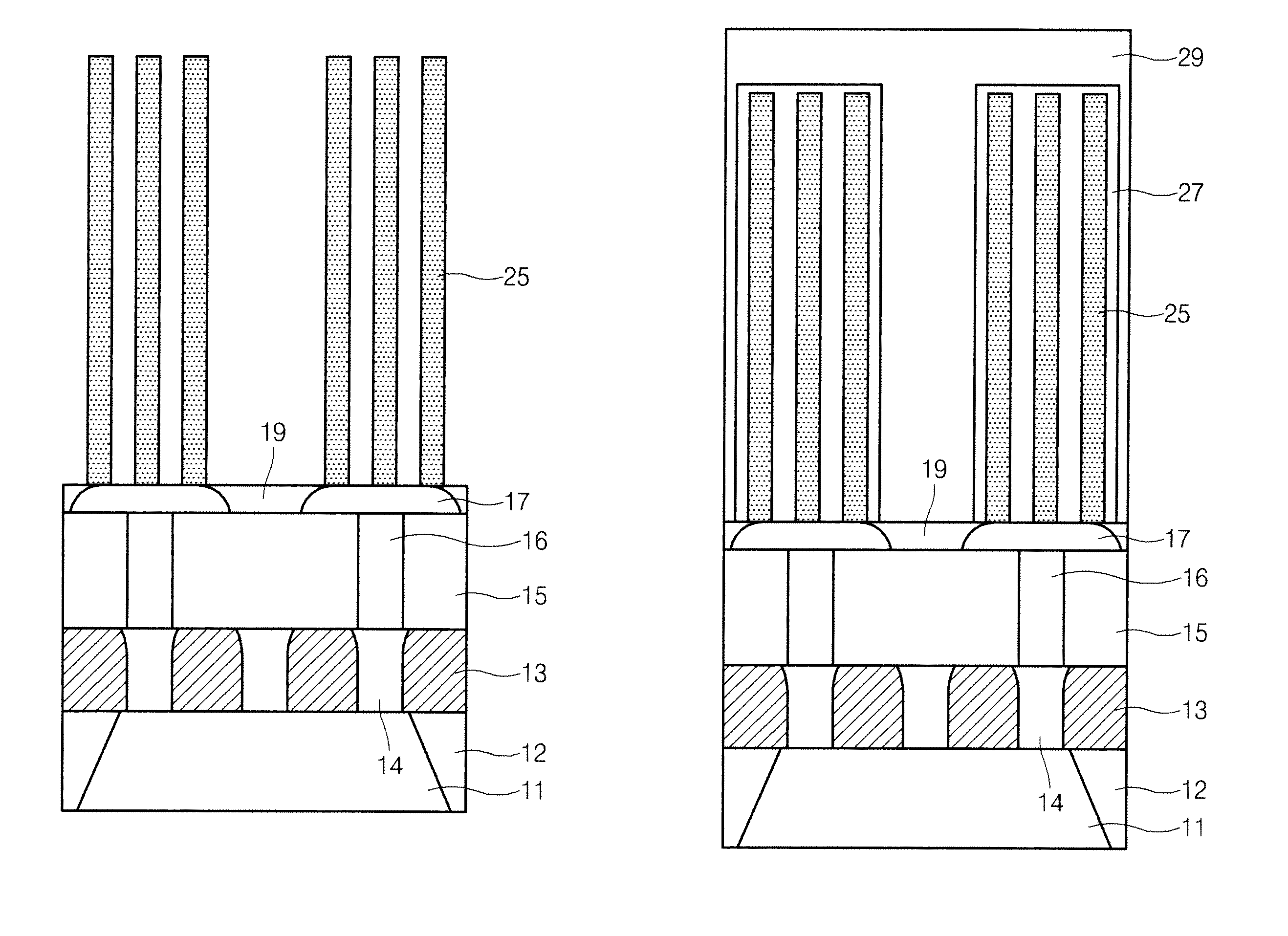
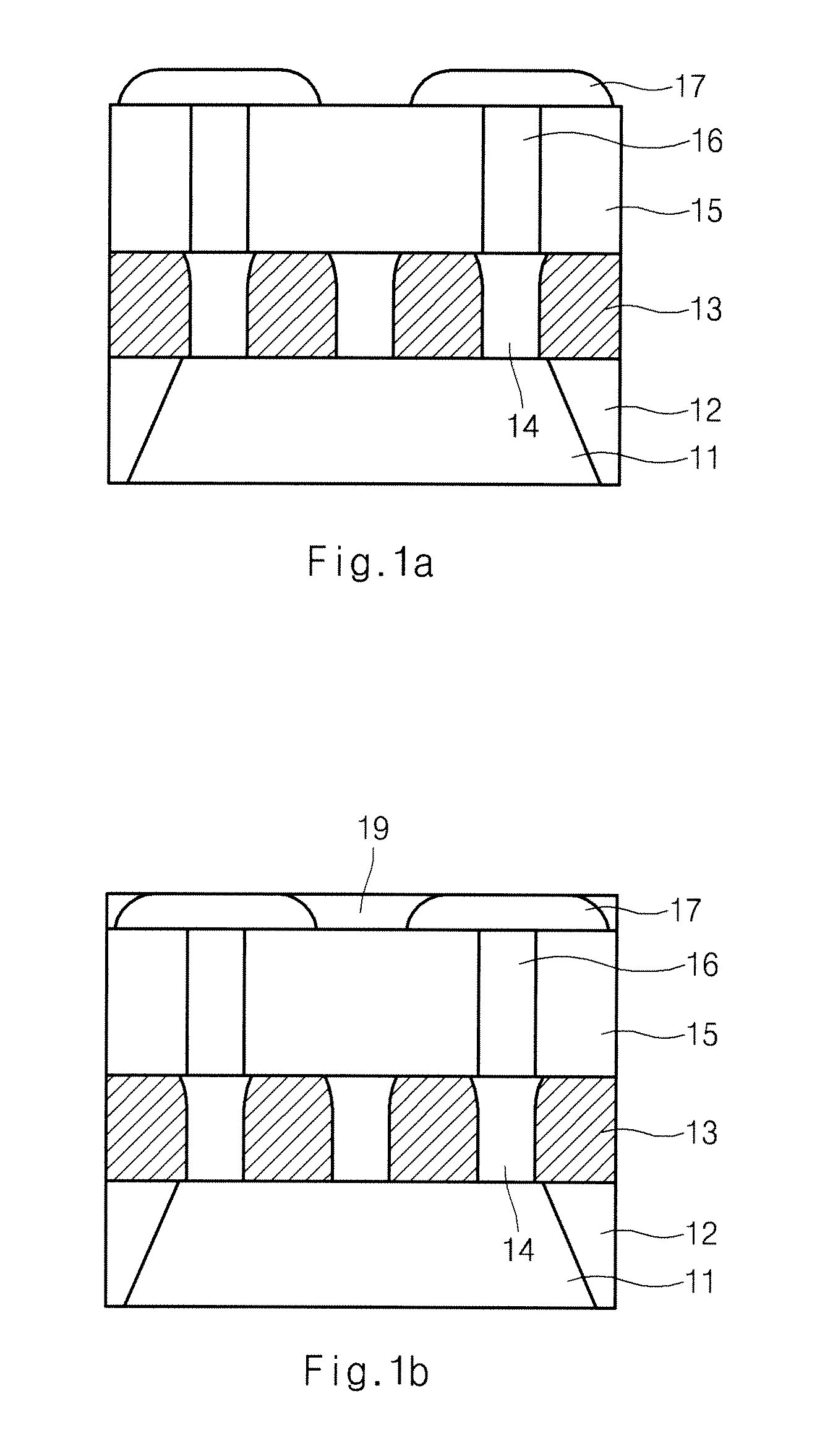
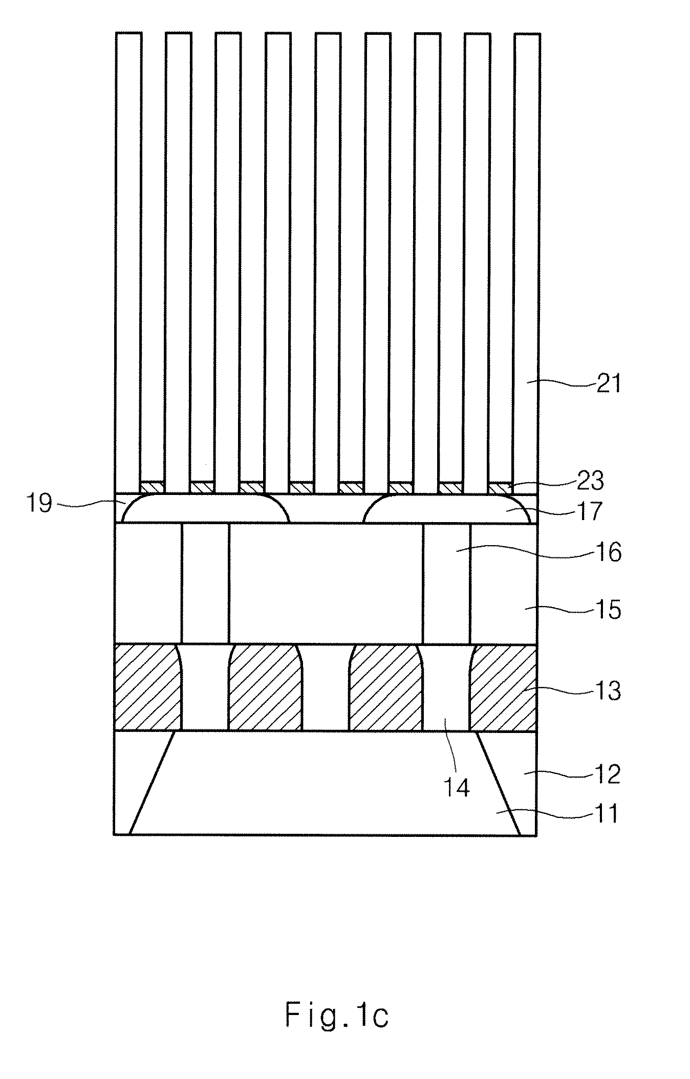
[0026]FIGS. 1a to 1f are cross-sectional diagrams illustrating a method for fabricating a capacitor of a semiconductor device according to an embodiment of the present invention.

[0027]Referring to FIG. 1a, a transistor including a gate electrode 13 and a landing plug contact 14 is formed over a substrate 11 including an isolation film 12.

[0028]A first insulating film 15 is deposited over the resulting structure including the gate electrode 13 and the landing plug contact 14. The first insulating film 15 is etched to form a via-contact 16 that exposes the landing plug contact 14.

[0029]A silicon in the landing plug contact exposed by the via-contact 16 is over-grown by an epitaxial process to fill a via-contact and to form a silicon layer 17 grown to the surface of the first insulating film 15. The over-grown silicon layer 17 is formed to have an island-type over the surface of the first insulating film 15. The silicon layer 17 is grown in a chamber, which is filled with a silicon gas...


PUM


Abstract

A method for fabricating a capacitor of a semiconductor device comprises forming a silicon nanowire structure having a large aspect ratio using a porous anodic alumina structure and applying the silicon nanowire structure to a bottom electrode, thereby obtaining a capacitor having secured capacitance.

Description

CROSS-REFERENCE TO RELATED APPLICATION[0001]Priority to Korean patent application number 10-2008-0088962, filed on Sep. 9, 2008, the entire disclosure of which is incorporated by reference, is claimed.BACKGROUND OF THE INVENTION[0002]The present invention relates to a method for fabricating a capacitor of a semiconductor device, and more specifically, to a method for fabricating a capacitor of a semiconductor device by forming a silicon nanowire structure having a large aspect ratio using a porous anodic alumina structure and applying the silicon nanowire structure to a bottom electrode, thereby obtaining a capacitor having secured capacitance.[0003]Due to rapid distribution of information media such as computers, the development of process equipment and process techniques is required to manufacture a high-integrated semiconductor memory device that operates at high speeds with large capacities.[0004]A memory cell of a DRAM device includes a transistor and a capacitor. The transisto...

Claims


Application Information

Patent Timeline
IPC IPC(8): H01L21/00
CPCB82Y10/00H01L27/10852H01L28/90H10B12/033H10B99/00H10B12/00
Inventor YOO, KEON
Owner SK HYNIX INC
Why Eureka
Try Eureka