
Circuit board manufacturing method and circuit board

a manufacturing method and circuit board technology, applied in the direction of conductive pattern formation, printed element electric connection formation, semiconductor/solid-state device details, etc., can solve the problems of large number of circuit boards, limited precision in alignment, and inability to form small holes around the whole outer periphery of holes, etc., to achieve the effect of easy manufacturing

Inactive Publication Date: 2010-03-16
SHINKO ELECTRIC IND CO LTD +1
View PDF11 Cites 3 Cited by
  • Summary
  • Abstract
  • Description
  • Claims
  • Application Information

AI Technical Summary

Benefits of technology

The patent text describes methods for manufacturing circuit boards using resin layers. The methods involve forming a first resin layer on a substrate with a conductive layer, and optionally a non-through hole or through hole in the substrate; adding a second resin layer on top of the first layer, with the second layer being insoluble or only slightly soluble in the developing solution for the first layer; removing the first layer of resin over the hole with the developing solution for the first layer; adding a third resin layer on the first layer at a circuit part and on the inner wall surface of the through hole or non-circuit part; removing the second and first resin layers; and etching the exposed portion of the conductive layer. The methods allow for precise placement of resin layers and efficient removal of unreacted resin layers. The resulting circuit boards have improved performance and reliability.

Problems solved by technology

However, there is a problem in that the hole and the land are not the concentric circles as shown in FIG. 100 when the alignment is not accurate.
Although the land is formed around the hole in the hole having the large land width in FIG. 100(b), the land is cut away by the hole portion in the hole having the small land width in FIG. 100(a), resulting in a problem of impossibility to form a hole having a small land around a whole outer periphery of the hole.
Under the conventional circumstance, the precision in the alignment has a limit due to precision in the perforation processing, the expansion of a substrate or a change in a dimension of a photomask for an exposure.
Moreover, the hole to be formed on the high density circuit board has a large number of diameters and the number of the holes is very large.
For these reasons, it has been very difficult to accurately carry out the alignment with respect to all the holes.
As described in JP-A-3-236956 and JP-A-7-7265, accordingly, the circuit design has a problem for employing a large land width regardless of the requirement of a landless hole or a hole having a small land width for the high density circuit board.

Method used


Image

  • Circuit board manufacturing method and circuit board
  • Circuit board manufacturing method and circuit board
  • Circuit board manufacturing method and circuit board

Examples


example

Example 1

Formation of First Resin Layer

[0242]By using a coating solution having a composition shown in Table 1, a resin film for a first resin layer (a thickness of the film after drying is 15 μm) formed by an alkali soluble resin was manufactured on a polyethylene terephthalate film having a thickness of 25 μm (manufactured by Mitsubishi Chemical Polyester Film Co., Ltd.) by using a curtain coating method.

[0243]

TABLE 1n-butyl methacrylate / n-butyl acrylate / 15parts by massmethacrylic acid copolymer (molecular weightof 20000, monomer composition ratio (mass) =4 / 3 / 3)dibutyl phthalate2.5parts by mass1-methoxy-2-propanol82.5parts by mass

[0244]As a circuit forming substrate, a copper-clad laminate including a copper foil having a thickness of 12 μm in a size of 200×200×0.4 mm was used to form a plurality of through holes having a diameter of 0.15 mm by means of a drill, and nonelectrolytic copper plating-electrolytic copper plating processings (OKUNO CHEMICAL INDUSTRIES CO., LTD., OPC Pro...

example 2

Formation of First Resin Layer

[0248]By using a coating solution having the composition shown in the Table 1, a resin film for a first resin layer (a thickness of the film after drying is 15 μm) formed by an alkali soluble resin was manufactured on a polyethylene terephthalate film having a thickness of 25 μm (manufactured by Mitsubishi Chemical Polyester Film Co., Ltd.) by using a curtain coating method.

[0249]As a circuit forming substrate, a copper-clad laminate including a copper foil having a thickness of 12 μm in a size of 200×200×0.4 mm was used to form a plurality of through holes having a diameter of 0.15 mm by means of a drill. Next, the first resin layer was laminated on the 120° C. preheating condition by using a laminator for a dry film. Then, a polyethylene terephthalate film was peeled at room temperature. Thereafter, heating was carried out at 80° C. for one minute to eliminate an unevenness of peeling and charging on the first resin layer which is generated by peeling...

example 3

Formation of First Resin Layer

[0253]By using a coating solution having the composition shown in the Table 1, a first resin layer (a thickness of the film after drying is 15 μm) formed by an alkali soluble resin was manufactured on a polyethylene terephthalate film having a thickness of 25 μm (manufactured by Mitsubishi Chemical Polyester Film Co., Ltd.) by using a curtain coating method.

[0254]A copper-clad laminate including a copper foil having a thickness of 12 μm in a size of 200×200×0.4 mm was used to form a plurality of through holes having a diameter of 0.15 mm by means of a drill, and nonelectrolytic copper plating-electrolytic copper plating processings (OKUNO CHEMICAL INDUSTRIES CO., LTD., OPC Process M) was executed to form a copper plated layer having a thickness of approximately 12.5 μm on a surface and internal walls of the through holes. Next, the first resin layer was thermo-compression bonded on the 120° C. preheating condition by using a laminator for a dry film. Th...


PUM


Abstract

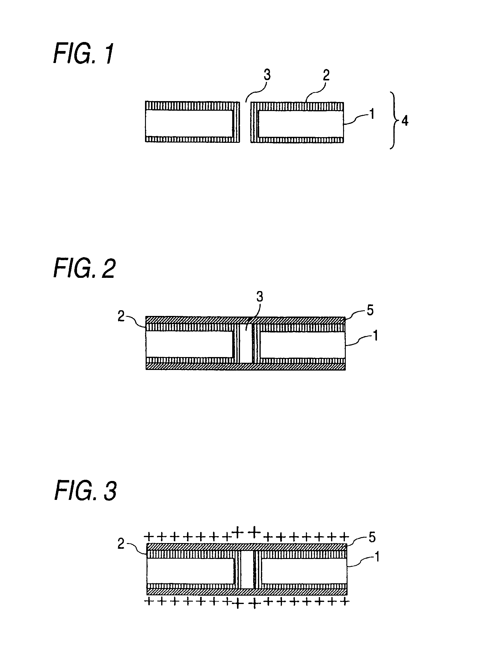
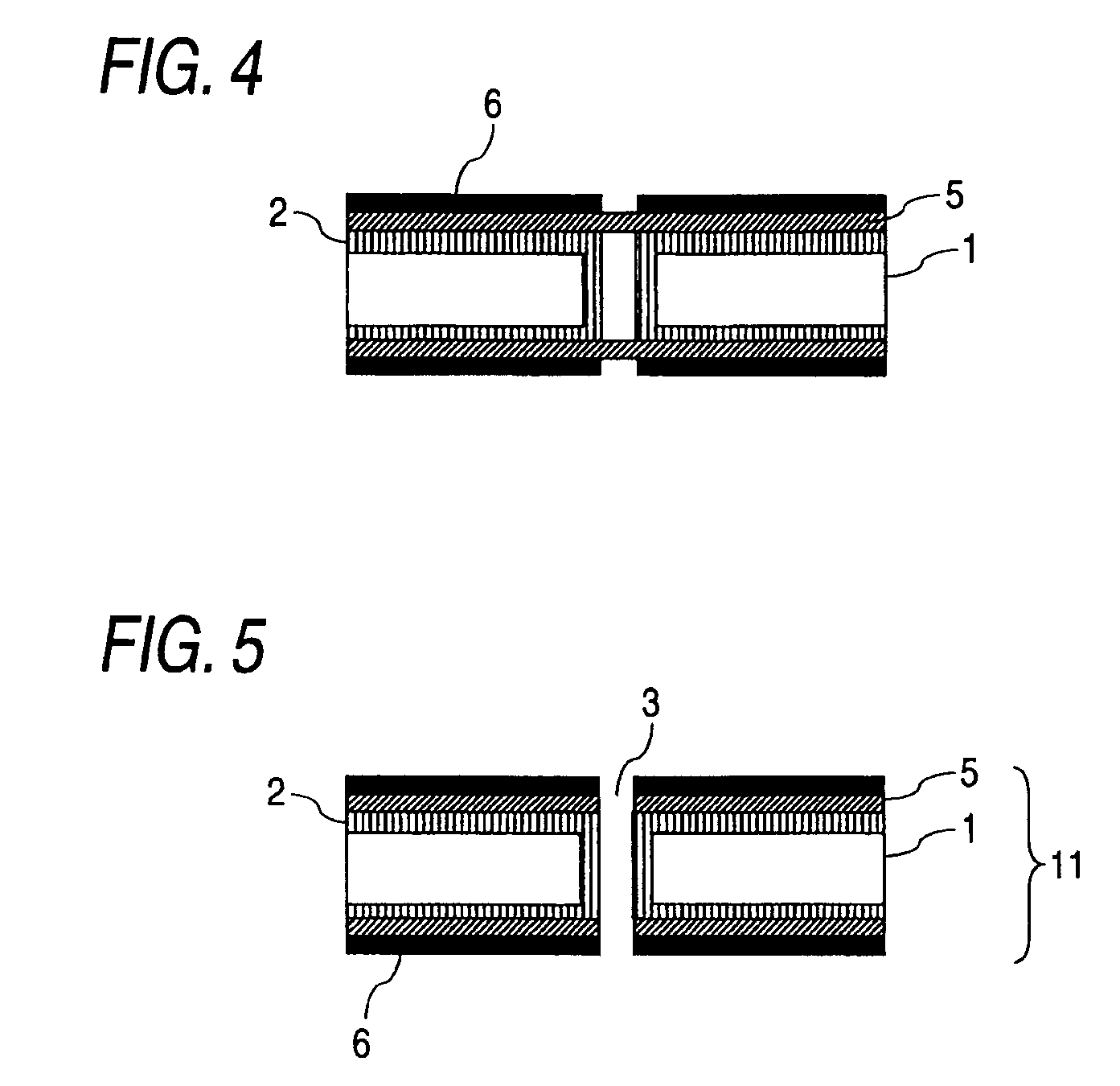
As means for solving a problem of a positional shift of a land and a hole which is caused by an alignment in the formation of an etching resist layer and a plated resist layer in a method of manufacturing a circuit board, there are provided a method of manufacturing a circuit board including the steps of forming a first resin layer on a surface of an insulating substrate having a conductive layer on the surface and an internal wall of a through hole or / and a non-through hole, forming a second resin layer which is insoluble or slightly soluble in a developing solution for the first resin layer on the first resin layer provided on the surface conductive layer, and removing the first resin layer provided over the hole with the developing solution for the first resin layer, and a method of manufacturing a circuit board including the step of uniformly charging a surface of the first resin layer to induce a potential difference to the first resin layer provided over the hole and the first resin layer provided on the surface conductive layer before forming the second resin layer. Moreover, there is provided a circuit board having a hole with a small positional shift and high precision.

Description

TECHNICAL FIELD[0001]The present invention relates to a method of manufacturing a circuit board, and more particularly to a method of manufacturing a circuit board having a hole, which is referred to as a through hole or a via hole, and a circuit board obtained by the manufacturing method thereof. In more detail, the invention relates to a method of manufacturing a circuit board for solving a problem of a positional shift between a land and a hole, which is caused by an alignment, and provides the method of manufacturing a circuit board which is adaptable to a landless hole or a hole with having the small land width, of which features are required for a high-density demand of a circuit board.BACKGROUND ART[0002]Referring to a recent trend for a down-sized or multifunctional electronic equipment, high-density or fine technology of the wiring pattern have been pursued for a circuit board. One of known means for achieving such condition is to form a circuit board in a multilayer. As sh...

Claims


Application Information

Patent Timeline
Patent Type & Authority Patents(United States)
IPC IPC(8): H01R12/04H05K1/00H05K1/11H05K3/00H05K3/06H05K3/10H05K3/42
CPCH05K1/116H05K3/0094H05K3/061H05K3/064H05K3/065H05K3/427H05K3/108H05K3/421H05K2201/09381H05K2201/09563H05K2201/09581H05K2201/098H05K2203/0517H05K2203/0577H05K2203/0582H05K2203/1184H05K2203/1394
Inventor FUKASE, KATSUYASAKAI, TOYOAKIIRISAWA, MUNETOSHIKOMURO, TOYOKAZUKANEDA, YASUONATSUKA, MASANORIAIZAWA, WAKANA
Owner SHINKO ELECTRIC IND CO LTD
Learn More