

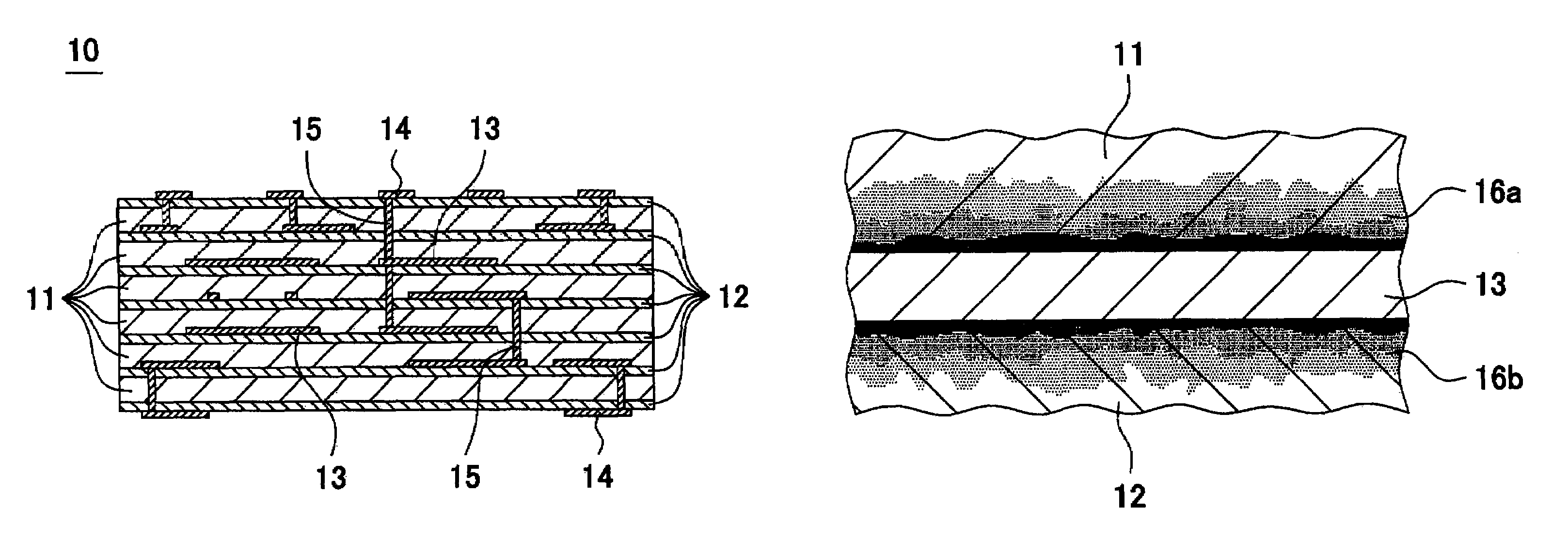
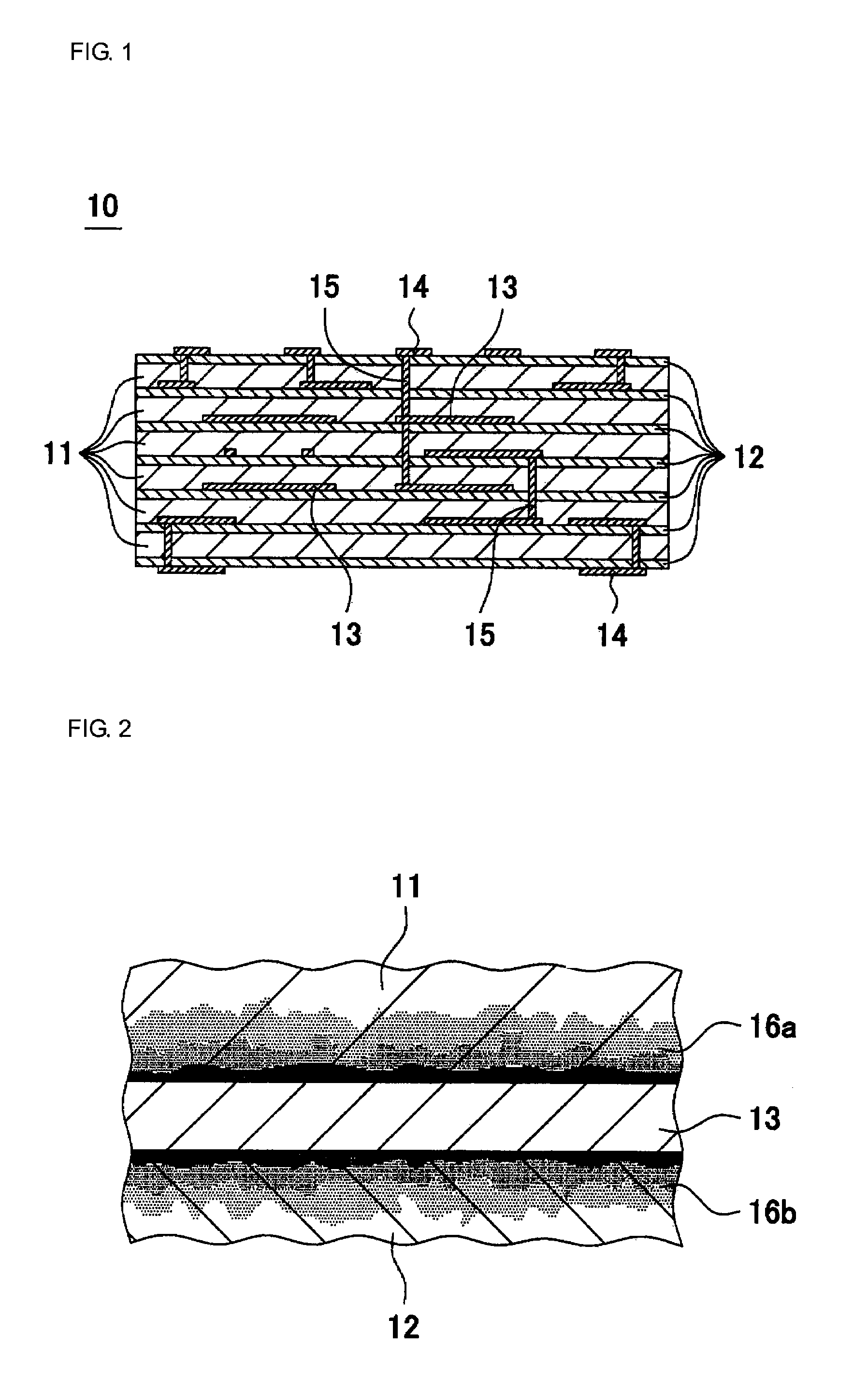
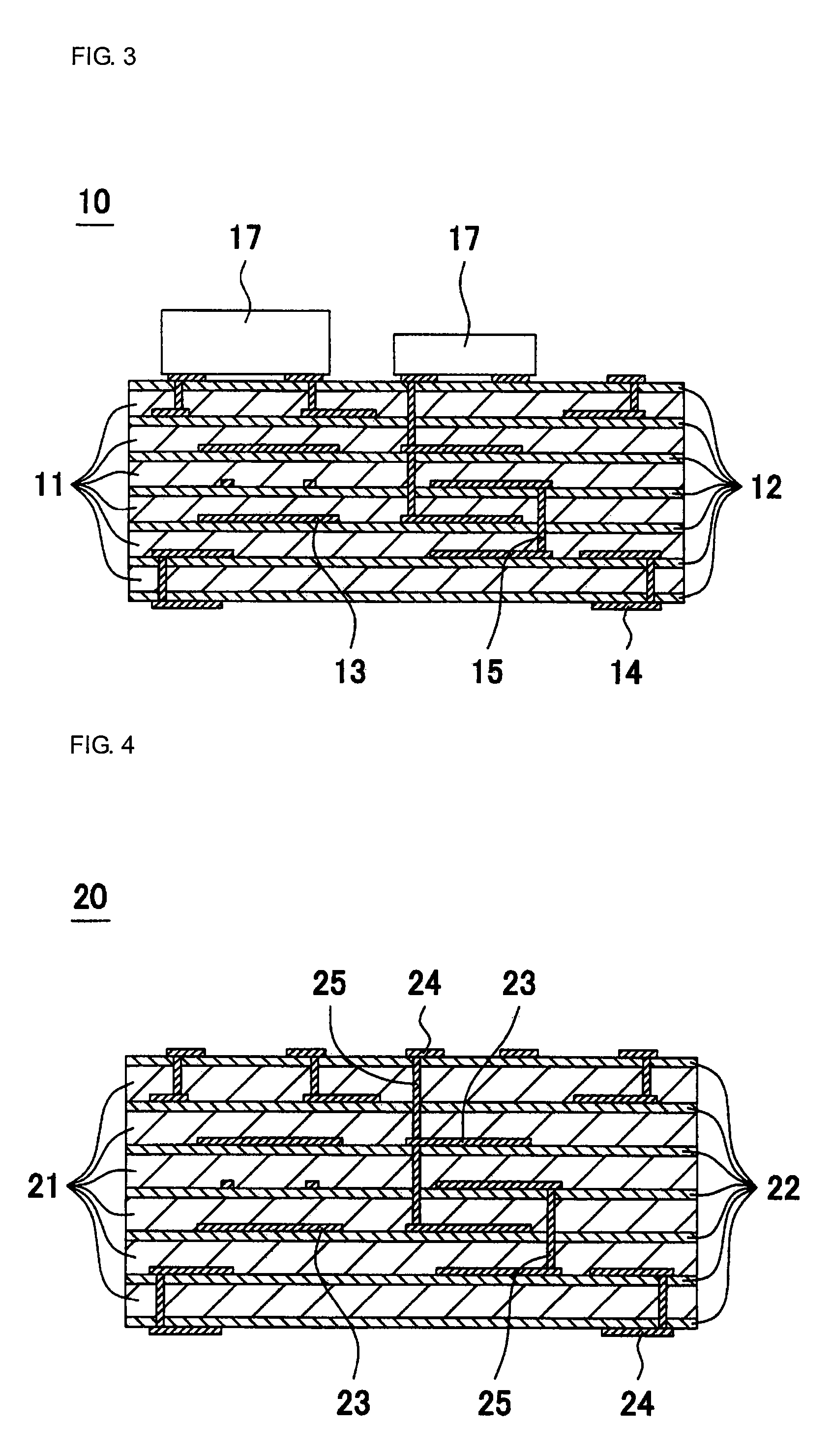
Ceramic multilayer substrate and method for manufacturing the same
a multi-layer substrate and ceramic technology, applied in the direction of ceramic layered products, metal adhesion improvement of the insulating substrate, transportation and packaging, etc., can solve the problems of internal conductor peeling and breakage reduce the warping of the first ceramic green layer, and reduce the occurrence of internal conductor peeling and breaking after firing
- Summary
- Abstract
- Description
- Claims
- Application Information
AI Technical Summary
Benefits of technology
Problems solved by technology
Method used
Image

Examples
experimental example 1
[0070]A Ba—Al—Si—O ceramic powder serving as a ceramic powder, toluene and a mixture of alcohols sold under the trademark EKINEN serving as a solvent, a butyral resin binder serving as a binder, and DOP (bis-2-ethylhexyl phthalate) serving as a plasticizer were prepared, and they were mixed so as to produce a ceramic slurry. The resulting ceramic slurry was molded into the shape of a sheet so as to produce a ceramic green sheet of 15.0 mm length, 15.0 mm width and 37 μm thickness.
[0071]An alumina powder, a B—Si—Ba glass powder, EKINEN serving as a solvent, a butyral resin binder serving as a binder, and DOP serving as a plasticizer were prepared, and they were mixed so as to produce a ceramic slurry. The resulting ceramic slurry was applied to the above-described ceramic green sheet, so as to produce a composite green sheet, in which a second ceramic green layer was formed on a first ceramic green layer, having a thickness of 40 μm was produced.
[0072]An electrically conductive paste...
experimental example 2
[0084]This experiment is intended to show that the phosphorus component has the function of restricting shrinkage of the ceramic green layer.
[0085]A ceramic green sheet containing a Ba—Al—Si—O ceramic powder was produced as in Experimental example 1.
[0086]A test paste including components in the proportion of 90 percent by weight of copper pyrophosphate, 1 percent by weight of ethyl cellulose serving as a binder, and 9 percent by weight of terpineol serving as a solvent was produced. The resulting test paste was applied all over one principal surface of the ceramic green sheet in such a way that the thickness became 10 μm, and firing was conducted under the conditions of a maximum temperature of 980° C. for 1 hour in a reducing atmosphere. The resulting substrate is called the first test substrate. A ceramic green sheet without the test paste, was fired under the same heat treatment condition as that of the first test substrate and called the second test substrate.
[0087]FIG. 8 is a ...
experimental example 3
[0090]This experiment is intended to show that the phosphorus component in the electrically conductive paste film has a function of restricting warp of the ceramic green layer.
[0091]A composite green sheet, in which a second ceramic green layer was formed on a first ceramic green layer, having a thickness of 40 μm was produced as in Experimental example 1.
[0092]An electrically conductive paste was produced as in Experimental example 1. The content of the copper pyrophosphate powder was as shown in Table 2.
[0093]The electrically conductive paste was printed on one first ceramic green layer in such a way that the thickness became 5 μm. A plurality of composite green sheets with no electrically conductive paste printed were laminated thereunder, and the first ceramic green layer with no electrically conductive paste printed was laminated thereunder. The resulting laminate was cut so as to produce a ceramic green laminate of 1 cm length, 1 cm width, and 0.36 mm thickness.
[0094]FIG. 10 i...
PUM
| Property | Measurement | Unit |
|---|---|---|
| thickness | aaaaa | aaaaa |
| thickness | aaaaa | aaaaa |
| thickness | aaaaa | aaaaa |
Abstract
Description
Claims
Application Information