Placement and routing of ECC memory devices for improved signal timing

a technology of memory devices and signal timing, applied in the field of memory for computer systems, can solve the problems of data stored in memory being corrupted, application or system crashes, and significant costs for a corporation, and achieve the effects of reducing delay, improving skew between dq, and reducing skew

Inactive Publication Date: 2010-04-13
RPX CORP
View PDF4 Cites 11 Cited by
  • Summary
  • Abstract
  • Description
  • Claims
  • Application Information

AI Technical Summary

Benefits of technology

[0008]There is a need for fulfilling timing requirements when interconnecting multiple DDR2 memory devices with ECC functionality to a controlling application-specific integrated circuit (ASIC) or network processor on a printed circuit board (PCB). There is also a need for managing skew between the data lines (DQ), data line strobes (DQS), clock signals (CLK), and address / command lines (ADDR / CMD) of a memory device to optimize timing results. Furthermore, there is a need for minimizing timing violations by balancing loads on each ADDR / CMD bit.
[0010]According to the forgoing, various exemplary embodiments minimize the skew between data lines, data line strobes, and address / command lines in a printed circuit board or integrated circuit. Thus, in various exemplary embodiments, data memory devices are arranged equidistant to a central location and oriented such that ADDR / CMD pins are closer to the memory controller than DQ / DQs pins. In various exemplary embodiments, ADDR / CMD signals that go to all RAM are routed through the central location, thereby reducing delay.
[0011]Accordingly, in various exemplary embodiments, this arrangement not only improves the skew between DQ and ADDR / CMD, but also makes it easier to balance an odd number of loads on ADDR / CMD signals, thereby achieving better signal integrity and timing. In addition, in various exemplary embodiments, DQ and DQs lines are routed in an indirect route, thereby further decreasing the skew between DQ and ADDR / CMD.

Problems solved by technology

Power surges, decay of the chip, and even cosmic rays originating in outer space can cause the data stored in memory to become corrupted.
In a typical memory chip, these errors go undetected, leading to application or system crashes.
For commercial applications in which data integrity is critical, such as web servers, these problems with reliability can result in significant costs to a corporation.
While ECC memory is an effective means for error detection and correction, the additional circuitry and data bits used to implement ECC memory introduce a number of problems.
Primarily, it becomes more difficult to implement synchronous dynamic random access memory (SDRAM) when including error correction circuitry.
If an operation is not performed in the proper time window, a timing violation occurs and often results in a system crash, the very problem ECC memory was designed to avoid.

Method used


Image

  • Placement and routing of ECC memory devices for improved signal timing
  • Placement and routing of ECC memory devices for improved signal timing
  • Placement and routing of ECC memory devices for improved signal timing

Examples


Embodiment Construction

[0020]In the detailed description that follows, reference is made to numerous embodiments of a “printed circuit board.” It should be understood that, as used herein, “printed circuit board” is not strictly limited to its ordinary meaning. Thus, in various exemplary embodiments, “printed circuit board” includes, but is not limited to, printed circuit boards, application-specific integrated circuits, hybrid integrated circuits, and other suitable replacements known to those of ordinary skill in the art.

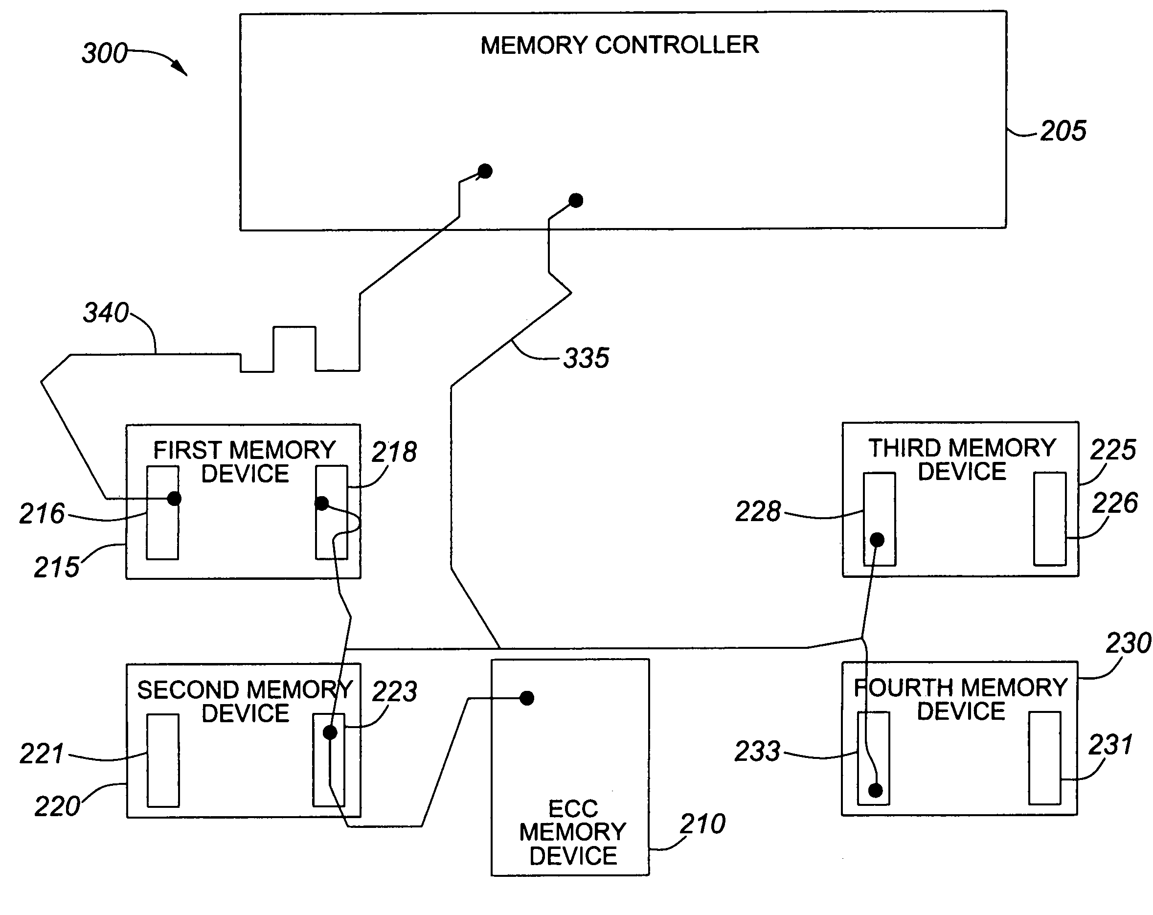
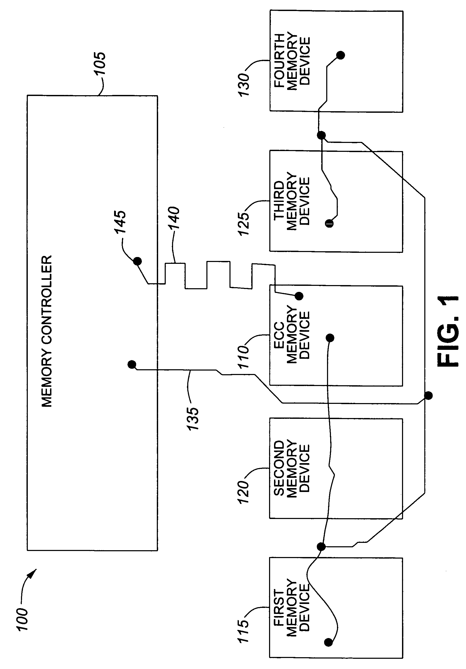
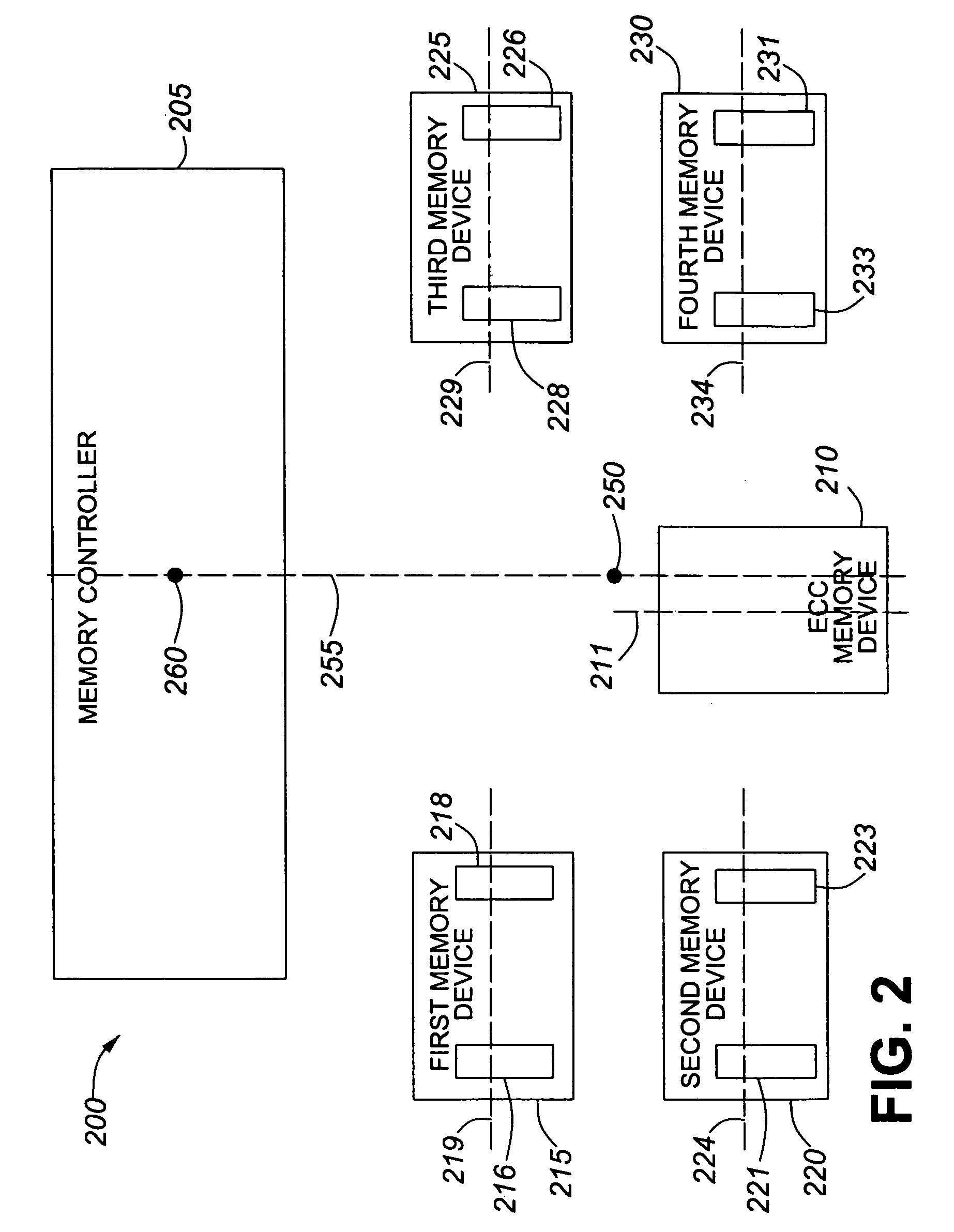
[0021]Referring now to the drawings, in which like numerals refer to like components or steps, there are disclosed broad aspects of various exemplary embodiments. FIG. 1 is a schematic diagram of a first exemplary embodiment of a printed circuit board 100 including four memory devices 115, 120, 125, 130 and an ECC memory device 110.

[0022]Exemplary printed circuit board 100 includes memory controller 105, ECC memory device 110, first memory device 115, second memory device 120, third mem...


PUM

PropertyMeasurementUnit
angleaaaaaaaaaa
timeaaaaaaaaaa
total lengthaaaaaaaaaa

Abstract

A printed circuit board may include a memory controller, a plurality of synchronous data memory devices, each synchronous memory device including at least one data pin and at least one address / command pin, an ECC memory device including at least one ECC data pin and at least one ECC address / command pin, and at least one surface. The plurality of synchronous data memory devices may be arranged around a central location on the at least one surface and each synchronous data memory device may be oriented such that the at least one data pin is further from the memory controller than the at least one address / command pin.

Description

BACKGROUND OF THE INVENTION[0001]1. Field of the Invention[0002]This invention relates generally to memory for computer systems.[0003]2. Description of Related Art[0004]A number of factors influence the likelihood of failure of Random Access Memory (RAM). Power surges, decay of the chip, and even cosmic rays originating in outer space can cause the data stored in memory to become corrupted. When a memory failure occurs, the byte of data returned from memory in response to a read request is different than the byte of data originally written into memory. In a typical memory chip, these errors go undetected, leading to application or system crashes. For commercial applications in which data integrity is critical, such as web servers, these problems with reliability can result in significant costs to a corporation.[0005]Error Correcting Code (ECC) memory addresses these problems by introducing additional circuitry for testing the accuracy of data as it passes in and out of memory. More ...

Claims


Application Information

Patent Timeline
Patent Type & Authority Patents(United States)
IPC IPC(8): G11C16/06
CPCG06F11/1044G11C5/025H05K1/181G11C5/04Y10T29/49002H05K2201/09254H05K2201/10159Y02P70/50
Inventor QU, PINGYUGAHAN, BARRIE PATRICK
Owner RPX CORP
Why Eureka
Try Eureka