Semiconductor device and manufacturing method thereof

a technology of semiconductors and manufacturing methods, applied in the direction of semiconductor devices, basic electric elements, electrical equipment, etc., can solve the problems of deteriorating an electrical characteristic of a tft, and achieve the effects of high current driving capacity, small variation of characteristics, and high speed operation

Inactive Publication Date: 2010-05-04
SEMICON ENERGY LAB CO LTD
View PDF62 Cites 49 Cited by
  • Summary
  • Abstract
  • Description
  • Claims
  • Application Information

AI Technical Summary

Benefits of technology

[0018]First, an insulating film (hereinafter, to be a cap film) is formed over a semiconductor film. A film thickness of this cap film is optimized so that the semiconductor film that is completely melted by laser beam irradiation is aligned in one plane orientation to grow a crystal. As the cap film, a material with which heat reaches the semiconductor film and which have enough transmittance to melt the semiconductor film is used. The cap film is preferably a solid and dense film. By forming the cap film, heat generated due to absorption of the laser beam in the semiconductor film can be efficiently utilized for crystallization, and laser crystallization can be performed with a lower energy density. It is considered that the cap film has an effect of suppressing decrease of viscosity of the melted semiconductor film, a reflection prevention effect, a thermal storage effect, or the like.
[0019]In addition, the laser beam irradiation is performed with an energy slightly higher than a lower energy density limit (hereinafter, to be referred to as E1) with which the semiconductor film of an irradiation region is completely melted. According to the present invention, the lowest limit of the laser beam energy is E1 because all that is needed is energy enough to completely melt the semiconductor film in the irradiation region. In addition, the uppermost limit is an energy with which a large grain crystal begins to be formed (hereinafter, to be referred to as E2). In other words, when an energy of a laser beam that can implement the present invention is regarded as E, the range of E is E1≦E≦E2. However, by suppressing the amount of heat given to the semiconductor film to the minimum necessary, a crystal nucleus can be prevented from generating more than necessary or the viscosity of the melted semiconductor film can be prevented from being decreased. Therefore, it is much preferable to adjust the range of the energy E of the laser beam with which irradiation is performed so as to satisfy E1≦E≦{(E1+E2) / 2} (FIG. 1A).
[0020]By controlling the energy of the laser beam in such a manner, turbulence of the semiconductor film due to heating can be decreased and stable crystal growth can be promoted. As shown in FIG. 1B, when a semiconductor film 03 having a cap film 04, which is formed over a substrate 01 and a base insulating film 02, is irradiated with a laser beam having an energy density of greater than or equal to E1 capable of completely melting the semiconductor film 03, quasi-single crystallization of the semiconductor film 03 is obtained and the plane orientation of crystal grains can be controlled.
[0041]According to the present invention, over an insulating substrate made from a material having a low melting point such as glass or plastic, it is possible to form a semiconductor film of a crystal having a large crystal grain size, in which the plane orientation between adjacent crystal grains are aligned in one direction or a direction that can be substantially regarded as one direction, that is, a quasi-single crystal that is infinitely close to a single crystal. Further, by using this quasi-single crystalline semiconductor film, it is possible to provide a semiconductor element capable of high speed operation with high current driving capacity and small variation of characteristics between elements, or a semiconductor device which is constituted by integrating a plurality of the semiconductor elements and a manufacturing method thereof.
[0042]Further, the quasi-single crystalline semiconductor film formed according to the present invention has extremely few crystal defects. By using this quasi-single crystal for an active layer of a TFT, a high-quality semiconductor device can be manufactured with high yields.
[0043]In addition, as shown in the present invention, by forming a cap film over a semiconductor film, heat generated due to absorption of a laser beam in the semiconductor film can be efficiently utilized for crystallization, and laser crystallization can be performed with a lower energy density. It is considered that this is because the cap film has a reflection prevention effect, a thermal storage effect, or the like. Therefore, when laser crystallization is performed to a semiconductor film with a cap film and a semiconductor film without a cap film by using laser oscillators having the same standard, a length of a linear beam spot can be more extended by using the semiconductor film with a cap film than using the semiconductor film without a cap film. Therefore, an area that can be crystallized per unit time can be increased, that is, throughput can be improved.

Problems solved by technology

However, the large grain crystal that is obtained by crystallization using the above laser has a feature that the plane orientation of crystal grain is totally different between adjacent large grain crystals, and the plane orientation of large grain crystal grains which are formed within an irradiation region of a laser beam is random and cannot be controlled to be one direction.
In addition, when each plane orientation is different between adjacent crystals, a trap level in a crystal grain boundary gets higher than a grain boundary in a case where the plane orientation is the same, thereby deteriorating an electrical characteristic of a TFT.

Method used


Image

  • Semiconductor device and manufacturing method thereof
  • Semiconductor device and manufacturing method thereof
  • Semiconductor device and manufacturing method thereof

Examples


embodiment 1

[0118]This embodiment will explain a measurement result of the plane orientation of a quasi-single crystalline silicon film of the present invention, which is used as a sample, by an EBSP method. In addition, the plane orientations of a single crystalline silicon film and a silicon film where a large grain crystal is formed were measured by an EBSP method in the same manner, and they were compared.

[0119]When an electron beam is made to enter a sample having a crystal structure, inelastic scatterings also occur at the back, and a linear pattern, which is peculiar to crystal orientation by Bragg diffraction, can also be observed in the sample. Here, this linear pattern has generally been referred to as a Kikuchi line. An EBSP method obtains crystal orientation of a sample by analyzing a Kikuchi line reflected in a detector.

[0120]A sample having a polycrystalline structure has crystal orientations where each crystal grain is different. Thus, every time the irradiation position of the s...

embodiment 2

[0177]This embodiment will explain a result of measuring characteristics of a semiconductor film of the present invention.

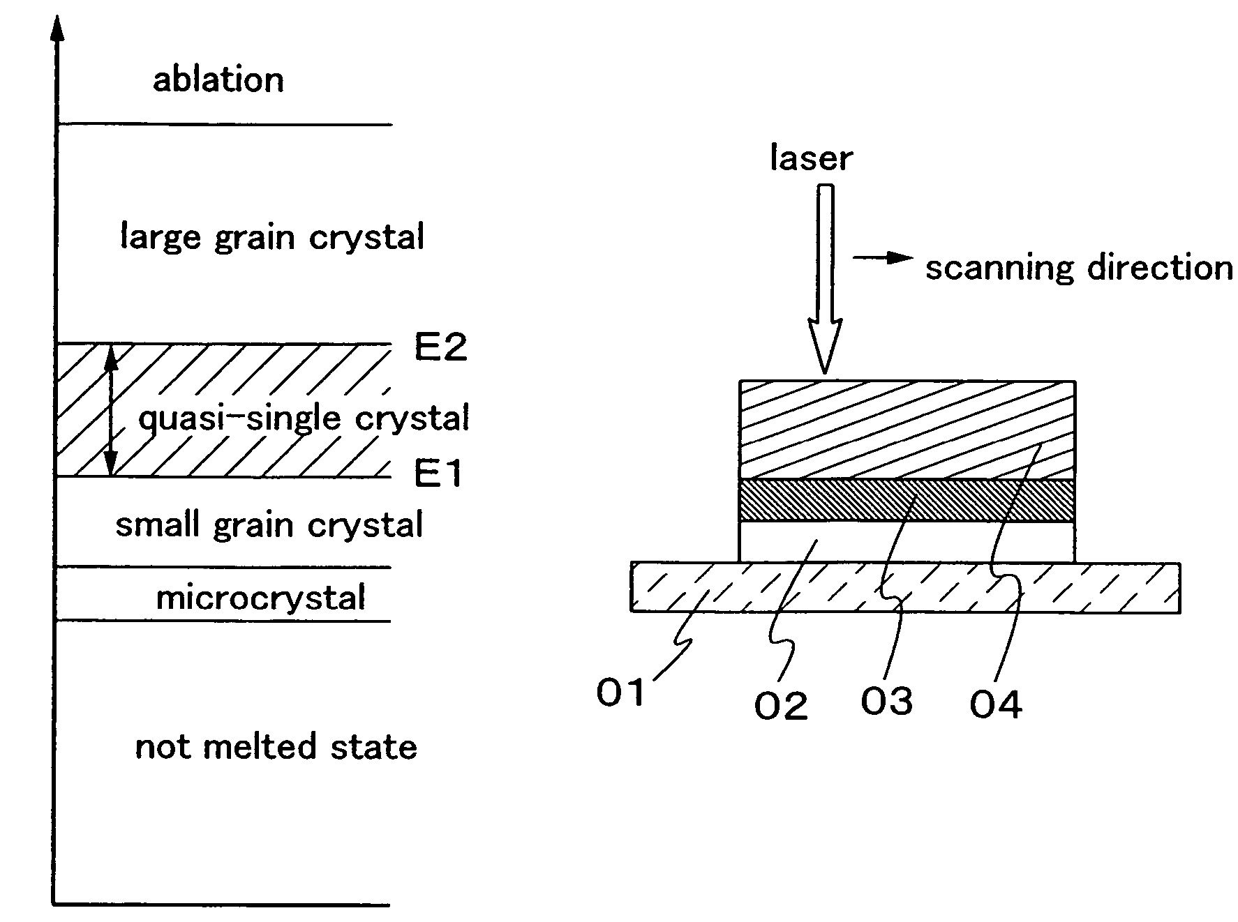
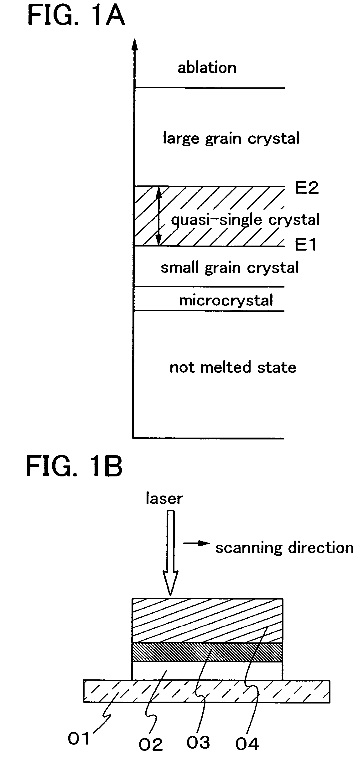
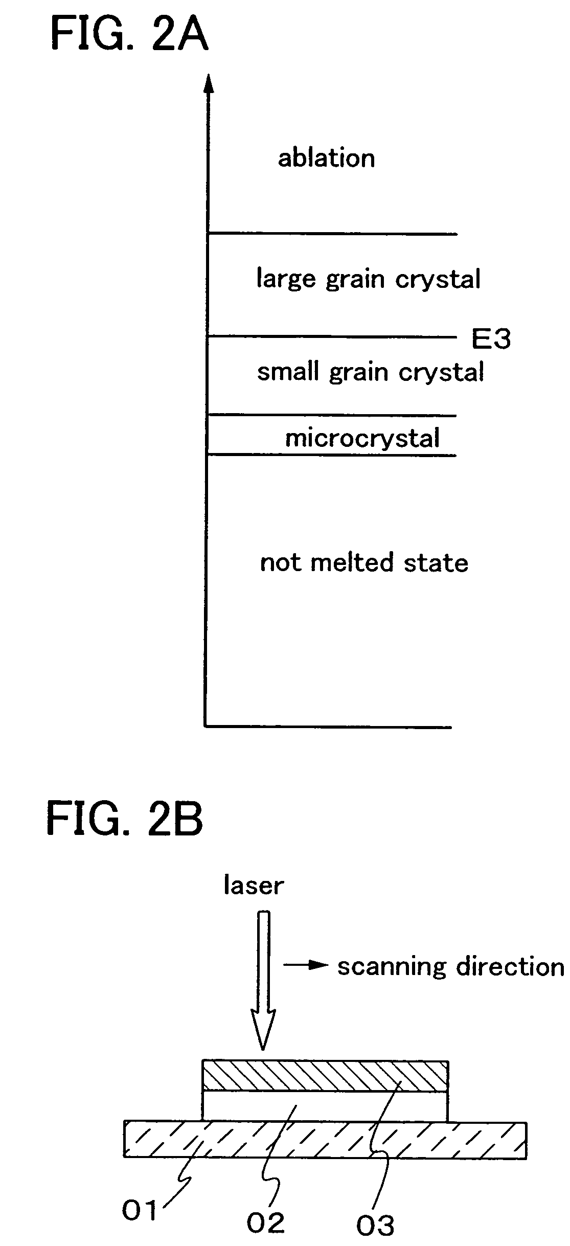
[0178]FIGS. 7A and 7B each show an optical microscope photograph of a quasi-single crystalline silicon film that is manufactured using the present invention. A sample was manufactured through the following procedure. A silicon oxide film containing nitrogen having a thickness of 150 nm was formed as a base insulating film over a glass substrate having a thickness of 0.7 mm, an amorphous silicon film was formed to have a thickness of 66 nm, and further a silicon oxide film containing nitrogen having a thickness of 500 nm was formed as a cap film. Next, two laser oscillators were prepared and each laser beam was emitted with an energy of 7.5 W. After synthesizing the energy of this two laser beams by using an optical system, the amorphous silicon film was irradiated with the laser beam through the cap film. The laser beam energy after synthesizing the laser beams a...

embodiment 3

[0186]A semiconductor film of the present invention was evaluated by Raman spectroscopy. Raman spectroscopy is one of effective methods to evaluate crystallinity of a substance, and is used in order to quantify the crystallinity of a semiconductor film which is formed by laser irradiation. Generally, a piece of information on crystallinity, a crystal grain size, or stress is obtained from a peak position or a full width at half maximum of a Raman line, and a piece of information on a plane orientation is obtained from intensity or the number of a Raman line. In addition, when the plane orientation of the manufactured film or crystal grains is unclear, a plane orientation or a crystal axis direction can be specified by carrying out polarization Raman measurement from a different orientation.

[0187]First, as shown in FIG. 11A, a glass substrate having a thickness of 0.7 mm is prepared as a substrate 300. A silicon oxide film containing nitrogen having a thickness of 150 nm was formed a...


PUM


Abstract

It is an object of the present invention to control the plane orientation of crystal grains obtained by using a laser beam, into a direction that can be substantially regarded as one direction in an irradiation region of the laser beam. After forming a cap film over a semiconductor film, the semiconductor film is crystallized by using a CW laser or a pulse laser having a repetition rate of greater than or equal to 10 MHz. The obtained semiconductor film has a plurality of crystal grains having a width of greater than or equal to 0.01 μm and a length of greater than or equal to 1 μm. In a surface of the obtained semiconductor film, a ratio of an orientation {211} is greater than or equal to 0.4 within the range of an angle fluctuation of ±10°.

Description

TECHNICAL FIELD[0001]The present invention relates to a technique for forming a semiconductor film having a crystalline structure by irradiating a semiconductor film with a laser beam and a semiconductor device such as a thin film transistor (hereinafter, a TFT) using, and the semiconductor film having a crystalline structure that is formed by using this technique. In addition, the present invention relates to a manufacturing method of the semiconductor device.BACKGROUND ART[0002]In recent years, a laser crystallization technique for forming a semiconductor film having a crystalline structure (hereinafter, a crystalline semiconductor film) by irradiating an amorphous semiconductor film which is formed over a glass substrate with a laser beam has been researched well. A crystalline semiconductor film is used because of high mobility as compared with an amorphous semiconductor film. Therefore, a TFT is formed using this crystalline semiconductor film, and such a TFT has been used for ...

Claims


Application Information

Patent Timeline
Patent Type & Authority Patents(United States)
IPC IPC(8): H01L21/84
CPCH01L21/2026H01L29/04H01L27/1292H01L27/1296H01L27/1266H01L27/1255H01L21/02683H01L21/02422H01L21/02488H01L21/02502H01L21/02609H01L21/0242H01L21/02672H01L21/0262H01L21/02425H01L21/02686H01L21/02678H01L21/02532H01L21/02595H01L21/02691H01L21/02675
Inventor MORIWAKA, TOMOAKI
Owner SEMICON ENERGY LAB CO LTD
Why Eureka
Try Eureka