Magnetic signal transmission line

a transmission line and signal technology, applied in the direction of magnetic bodies, magneticonductor/solid-state device details, instruments, etc., can solve the problems of limiting the degree of integration in the semiconductor integrated circuit, and the current technology of the integrated circuit cannot achieve the transmission line width as small as 100 nm or less, so as to achieve a higher transmission rate and small width

Inactive Publication Date: 2010-05-25
NEC CORP
View PDF13 Cites 3 Cited by
  • Summary
  • Abstract
  • Description
  • Claims
  • Application Information

AI Technical Summary

Benefits of technology

[0007]It is an object of the present invention to provide a new signal transmission line capable of being fabricated to have a smaller width as small as 100 nm or less and having a transmission rate which is higher compared to that achieved by the current technology.
[0010]The magnetic signal transmission line of the present invention is free from the problem encountered in the conventional signal transmission line wherein the signal transmission rate is limited by the CR constant, and has an advantage that the width of the signal transmission line can be made as small as 100 nm or less.

Problems solved by technology

In addition, a signal transmission line having a width as small as 100 nm or less is not achieved by a current technology for the integrated circuit.
This limits the degree of integration in the semiconductor integrated circuit.

Method used


Image

  • Magnetic signal transmission line
  • Magnetic signal transmission line
  • Magnetic signal transmission line

Examples


first embodiment

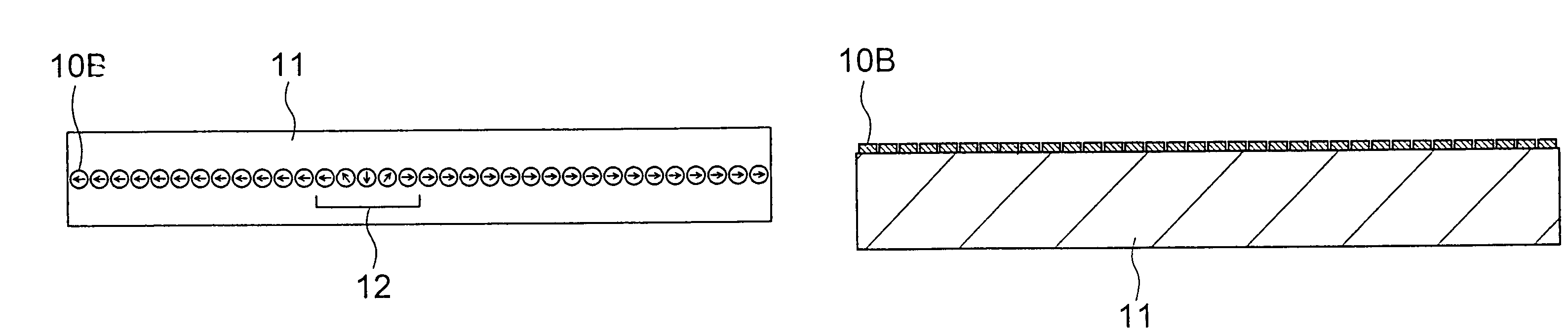
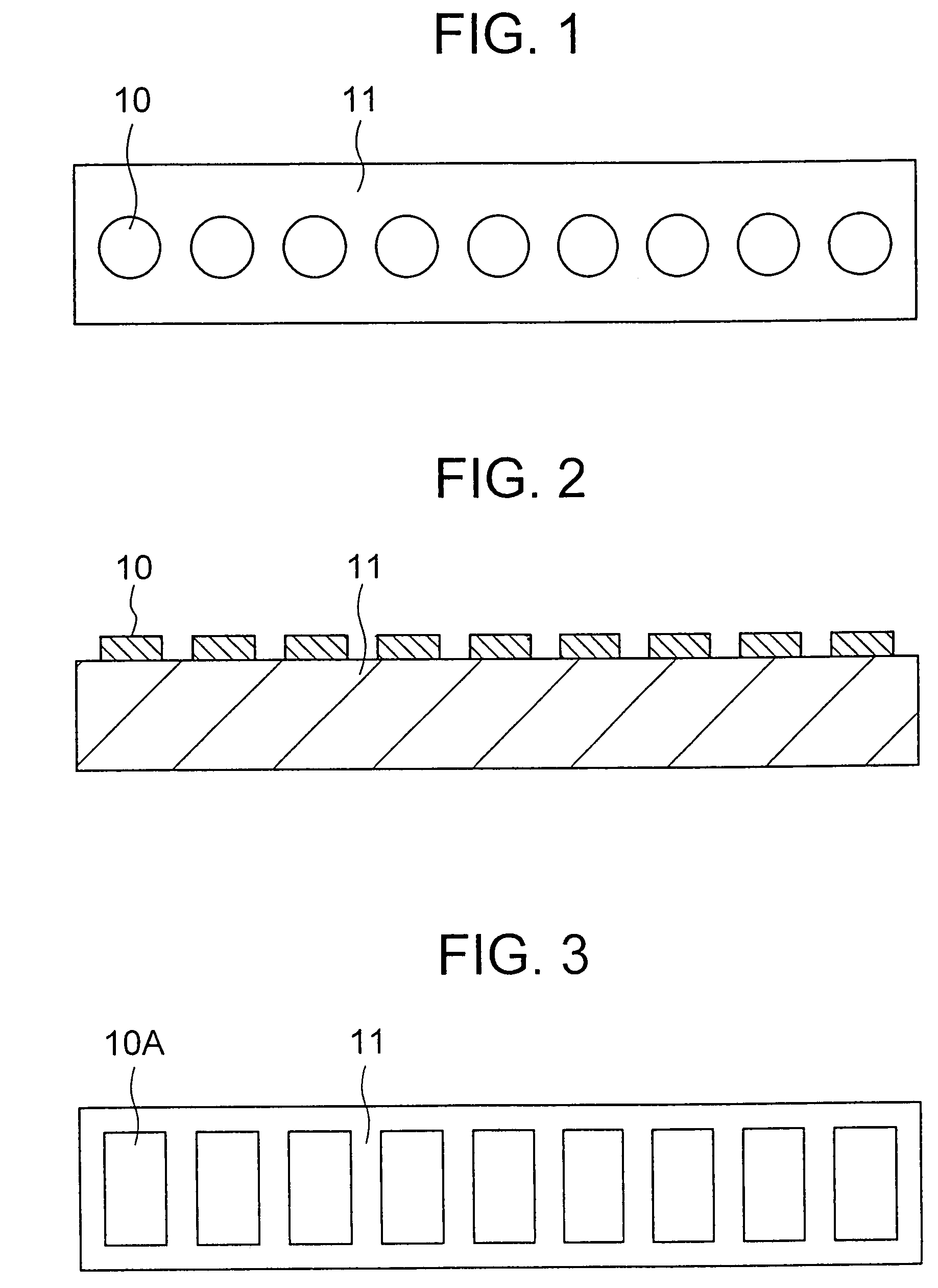
[0030]Referring to FIGS. 1 and 2, a magnetic signal transmission line according to the present invention includes a silicon substrate 11, and a one-dimensional array of magnetic dots 10 formed on the main surface of the silicon substrate. The array includes about 10,000 magnetic dots (minute ferromagnetic bodies) 10 in this embodiment. The magnetic dots 10 are made of iron and formed by the steps of forming a resist film on the silicon substrate, exposing the resist film for patterning using an electron beam exposure technique, sputtering iron onto the silicon substrate by using the resist film as a mask, and removing the resist film from the silicon substrate.

[0031]Each magnetic dot 10 is of a column shape having a diameter of 20 nm and a height of 10 nm. The distance between adjacent two of the magnetic dots 10 is 10 nm. Since the thickness of the magnetic wall of a bulk of iron is about 30 nm, the magnetic dot 10 having those dimensions, smaller than 30 nm, has a single-magnetiza...

third embodiment

[0034]In the signal transmission line according to the present embodiment, the magnetic moment of each magnetic dot assumes a minimum due to the interactive energy when the magnetization is aligned with the direction of the array. If the magnetic signal transmission line is subjected to rotation of the magnetization of one or some of the magnetic dots, as shown at the location 12, the rotation of the magnetization can be transferred as a solitary wave at a high speed in the direction of the array. The transmission rate of the solitary wave can be calculated from the distance between the dots, the height of the dot and the saturation magnetization of iron. The calculated rate is 100 m / s in the

[0035]The transmission rate 100 m / s itself is not very large compared to the transmission rate in a conventional signal line. However, considering that the magnet signal line has a very small length due to its high-density-integration capability, and that a number of solitary waves can be transm...


PUM

PropertyMeasurementUnit
widthaaaaaaaaaa
heightaaaaaaaaaa
diameteraaaaaaaaaa

Abstract

A magnetic signal transmission line includes a one-dimensional array of a plurality of single-magnetization domains each formed in a ferromagnetic body. The anisotropic energy of the single-magnetization domains is zero to 120% of the interactive energy acting between dipoles in adjacent single-magnetization domains. The single-magnetization domains are formed by sputtering iron onto a silicon substrate by using a mask.

Description

BACKGROUND OF THE INVENTION[0001](a) Field of the Invention[0002]The present invention relates to a magnetic signal transmission line and, more particularly, to a magnetic signal transmission line for transmitting a signal through a one-dimensional array of a plurality of single-magnetization domains.[0003](b) Description of a Related Art[0004]Metallic interconnects, such as copper and aluminum interconnects, or low-resistance polysilicon interconnects are generally used in an electronic circuit for signal transmission. The transmission rate in the signal transmission by using the metallic interconnects or polysilicon interconnects is restricted by a delay constant (CR constant) of the interconnect, the CR constant being defined by the product of the resistance R by the parasitic capacitance C of the interconnect. The CR constant is currently a primary factor limiting the transmission rate in a smaller-size electronic circuit.[0005]More specifically, signal transmission on the order...

Claims


Application Information

Patent Timeline
Patent Type & Authority Patents(United States)
IPC IPC(8): H01L41/12H01L43/02H01L43/12H01F1/00H01P3/00
CPCB82Y25/00H01P3/00H01F1/0072
Inventor ISHIZAKA, SATOSHINAKAMURA, KAZUO
Owner NEC CORP
Why Eureka
Try Eureka