SPM cantilever and manufacturing method thereof

a manufacturing method and cantilever technology, applied in the direction of mechanical measuring arrangements, mechanical roughness/irregularity measurements, instruments, etc., can solve the problems of difficult control of the angle and/or direction of cnt, difficult to meet such requirements, and difficult to form a probe with reproducible cnt, etc., to achieve excellent reproducibility, easy to form, and well controlled

Active Publication Date: 2010-06-15
OLYMPUS CORP
View PDF13 Cites 8 Cited by
  • Summary
  • Abstract
  • Description
  • Claims
  • Application Information

AI Technical Summary

Benefits of technology

[0012]Such construction makes it possible to achieve SPM cantilever capable of stable, high-resolution measurements with having high reliability and excellent durability.
[0016]With the construction of SPM cantilever according to the second to fourth aspects, the structure and / or characteristics of the thin line may be selectively used in agreement with its use. Also, since the resulting probe has a high aspect ratio, high-resolution measurements are possible. Especially in the case of CNF, CNT, or GNF, high-resolution measurements with excellent durability are made possible. In the case of SNW or SNT, a prior-art SPM cantilever made of silicon may be used without change in construction. The case of using MNW or MNT makes it possible to achieve SPM cantilever having electrical conductivity or ferromagnetism.

Problems solved by technology

It is becoming difficult to meet such requirements by those scanning probe microscopes using a conventional Si-made cantilever that is available on market.
Furthermore it is difficult to control the angle and / or direction at which CNT 103 is attached to the probe terminal end portion 101a and the forming of a probe with a reproducible CNT is also difficult because of the one-by-one work to be done.
In this case, although growth / formation of a large quantity of CNT is possible, the selective forming of a piece of CNT from the probe terminal end portion with controlling the direction of its growth is very difficult.
Especially the CNT occurring from the sides of the probe has an adverse effect for example on AFM measurements.

Method used


Image

  • SPM cantilever and manufacturing method thereof
  • SPM cantilever and manufacturing method thereof
  • SPM cantilever and manufacturing method thereof

Examples


second embodiment

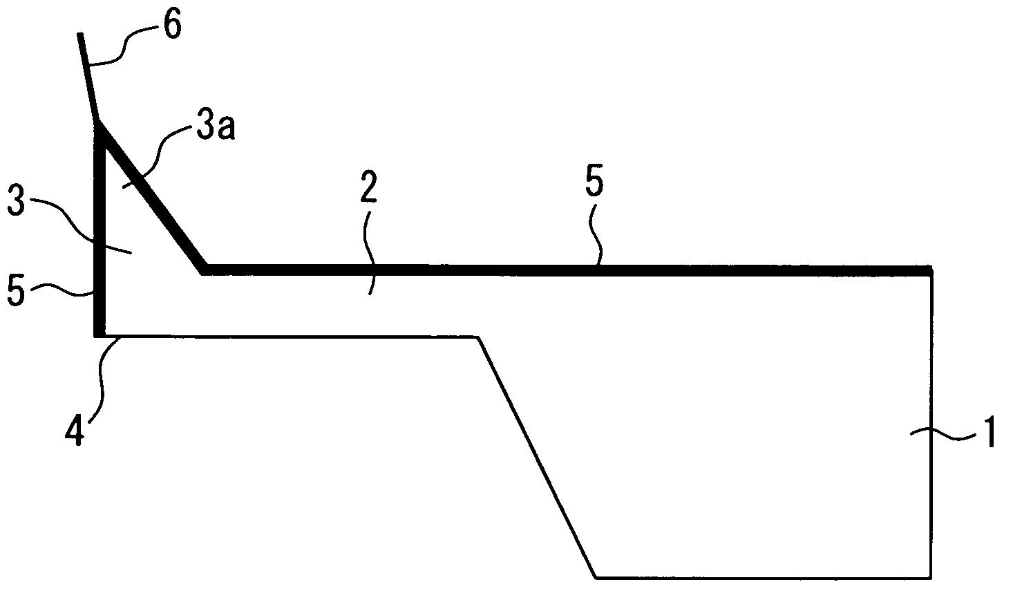
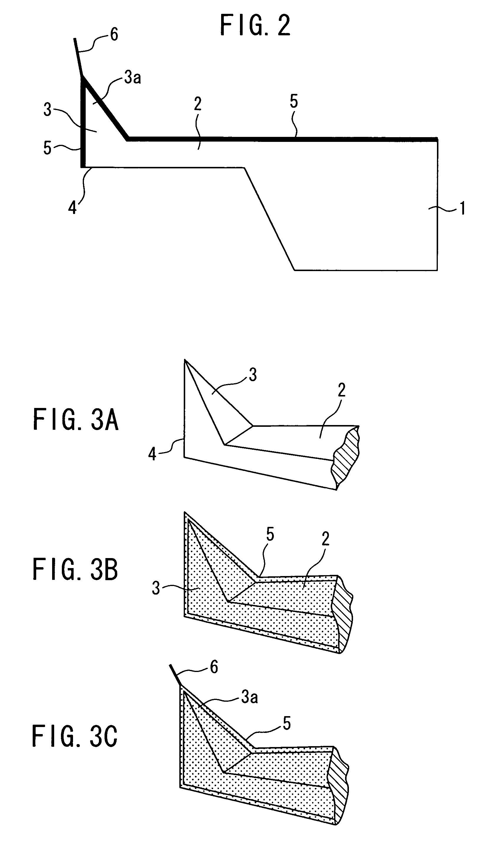
[0058]the invention will now be described. FIG. 7 is a side view showing construction of SPM cantilever according to the present embodiment. FIG. 7 includes: a support portion 1 fabricated by processing a single crystal silicon wafer; a lever portion 2 extended from the support portion 1; and a probe 3 disposed toward a free end 4 of the lever portion 2. What is denoted by numeral 7 is a graphite film which is a carbon compound, formed only at a probe terminal end portion 3a, and 8 is a piece of carbon nanofiber (CNF) thin line formed at the probe terminal end portion 3a, grown / formed from the graphite film 7.

[0059]A manufacturing method of SPM cantilever having CNF thin line at the probe terminal end portion according to the present embodiment will now be briefly described by way of FIG. 8A to FIG. 8J. First, as shown in FIG. 8A, an SOI (Silicon-On-Insulator) silicon substrate 21 having lattice plane (100) is prepared, and a mask pattern 22 for forming the support portion of the ca...

first embodiment

[0068]Finally, similarly to the manufacturing method of the first embodiment, the interior of a vacuum apparatus is set to a vacuum of the order of 10−2 Pa to 10−8 Pa and preferably of the order of 10−3 Pa to 10−5 Pa, and argon ion, which is a rare gas ion, is used as the source of ionization. An acceleration voltage of 0.1 to 300 keV and an average ionic current density of 2 μA / cm2 to 10 mA / cm2 are employed to achieve an ion beam sputter rate of the order of 2 nm to 1 μm / min so as to grow / form CNF thin line having a length of the order of 0.1 to 10 μm and a thickness of the order of 1 to 10 nm from the probe terminal end portion by means of an ion irradiation of 1 to 100 minutes at room temperature. When the ion beam is irradiated onto the probe terminal end portion in this manner, chemical bond and transfer occur of the atoms at the probe terminal end portion, and as a result a piece of thin line consisting of CNF is selectively grown / formed at the probe terminal end portion.

[0069...


PUM


Abstract

An SPM cantilever of the present invention including: a support portion (1) fabricated by processing a single crystal silicon wafer; a lever portion (2) formed in a manner extended from the support portion; a probe (3) disposed at a free end side of the lever portion; a coating of graphite film (5) covering all over the side on which the probe is formed and the entire probe; and a piece of thin line (6) consisting of a carbon nanofiber (CNF) or carbon nanotube (CNT) or graphite nanofiber (GNF) grown / formed from the graphite film at a probe terminal end portion (3a).

Description

TECHNICAL FIELD[0001]The present invention relates to SPM cantilevers for use in a scanning probe microscope (SPM), and more particularly relates to SPM cantilever with an improved probe portion and manufacturing method thereof.BACKGROUND OF THE INVENTION[0002]The scanning probe microscopes (SPM) have a measuring resolution of atomic order and are used in various fields such as surface configuration measurements. A scanning probe microscope maintains a distance of the order of nanometer between its probe and a sample so that fine configurations be measured by detection of a physical quantity such as tunneling current or atomic force that occurs between the probe and the sample. Among others, an atomic force microscope (AFM) is suitable for high-resolution detection of the sample surface configuration and is used in measurements of surface configuration of semiconductors, optical disks, biological samples, etc.[0003]The requirements for such scanning probe microscopes have recently b...

Claims


Application Information

Patent Timeline
Patent Type & Authority Patents(United States)
IPC IPC(8): G01B5/28G01Q60/16G01Q60/24G01Q60/32G01Q60/38G01Q70/12G01Q70/16
CPCB82Y15/00B82Y35/00G01Q70/12Y10S977/849Y10S977/86
Inventor KITAZAWA, MASASHIOTA, RYOTANEMURA, MASAKI
Owner OLYMPUS CORP
Why Eureka
Try Eureka