Gallium nitride-based compound semiconductor light-emitting device
a compound semiconductor and light-emitting device technology, applied in the direction of semiconductor devices, basic electric elements, electrical apparatus, etc., can solve the problems of high contact resistance, low operating voltage, high resistance in diffusion direction, etc., to achieve good crystallinity of semiconductors, reduce contact resistance between semiconductors and transparent electrically conducting film layers, and reduce the effect of resistan
- Summary
- Abstract
- Description
- Claims
- Application Information
AI Technical Summary
Benefits of technology
Problems solved by technology
Method used
Image
Examples
example 1
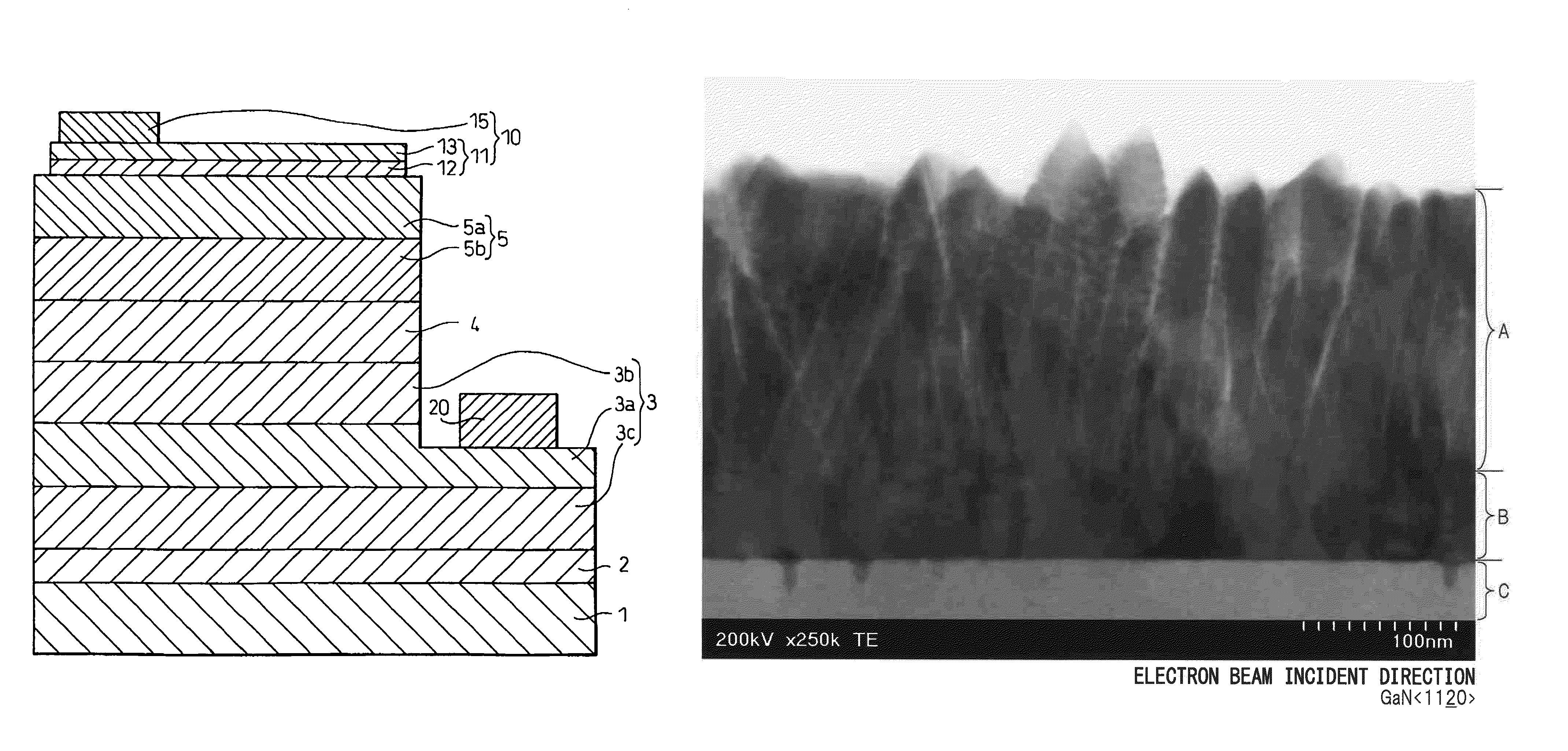
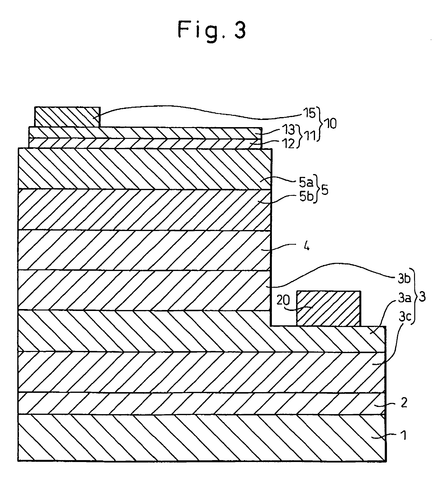
[0079]FIG. 3 is a schematic view showing the cross-section of a gallium nitride-based compound semiconductor light-emitting device produced in this Example, and FIG. 4 is a schematic view showing the planar surface thereof. An n-type semiconductor layer (3) consisting of a 3 μm-thick underlying layer (3c) composed of undoped GaN, a 2 μm-thick n-type contact layer (3a) composed of Si-doped n-type GaN and a 0.03 μm-thick n-type clad layer (3b) composed of n-type In0.1Ga0.9N, a light-emitting layer (4) having a multi-quantum well structure in which a 0.03 μm-thick barrier layer composed of Si-doped GaN and a 2.5 nm-thick well layer composed of In0.2Ga0.8N were stacked five times and the barrier layer was finally provided, and a p-type semiconductor layer (5) consisting of a 0.05 μm-thick p-type clad layer (5b) composed of Mg-doped p-type Al0.07Ga0.93N and a 0.15 μm-thick p-type contact layer (5a) composed of Mg-doped p-type GaN were sequentially stacked on a sapphire substrate (1) thro...
examples 2 and 3
[0091]Gallium nitride-based compound semiconductor light-emitting devices were produced in the same manner as in Example 1 except for changing the film formation condition of the positive electrode (the pressure of the sputtering apparatus at the formation of the transparent electrically conducting film contact layer), and the device characteristics were evaluated. The results obtained are shown in Table 1 together with the results of Example 1. Incidentally, in these light-emitting devices, the thickness of the positive electrode metal mixed layer was from 1 to 5 nm, and the proportion of the positive electrode metal was from 0.5 to 18%. As for the semiconductor metal mixed layer, these are shown in Table 1.
[0092]
TABLE 1Pressure atFormation ofSemiconductor Metal Mixed LayerTransparentProportion of Semiconductor Metal [at. %]Device CharacteristicsElectricallyPortion of 1 nm fromPortion of 3 nm fromForwardLightconducting FilmThicknessp-Type Contact Layerp-Type Contact LayerVoltageEmi...
example 4
[0093]A gallium nitride-based compound semiconductor light-emitting device was produced in the same manner as in Example 1 except for not performing the heat treatment after the formation of the positive electrode. Its device characteristics are shown also in Table 1.
PUM
 Abstract
Description
Claims
Application Information


