CMOS integration scheme employing a silicide electrode and a silicide-germanide alloy electrode

a technology of silicide electrodes and alloy electrodes, applied in the field of silicide electrodes and silicide alloy electrodes, can solve the problems of interfacial defects between a channel and the gate dielectric, the difficulty of integrating metal gate electrodes into a semiconductor structure employing cmos transistors, and the difficulty of integrating metal gate electrodes into the semiconductor structure,

Inactive Publication Date: 2010-07-06
IBM CORP
View PDF14 Cites 7 Cited by
  • Summary
  • Abstract
  • Description
  • Claims
  • Application Information

AI Technical Summary

Benefits of technology

[0010]In order to reduce processing complexity and cost, a self-aligned metal gate processing scheme employing a sacrificial layer is disclosed. The sacrificial layer comprises a germanium-containing layer. This processing flow allows for high temperature processing for source and drain activation anneals without concern for reaction between a high-k-gate dielectric and a metal gate material. Self-aligned silicide portions, including a filly silicided metal silicide gate electrode, are formed on one type of transistor, which is typically an n-type field effect transistor, while self-aligned metal silicide-germanide alloy portions, including a fully metallized silicide-germanide alloy gate electrode, are formed on another type of transistor. The present invention avoids full implementation of replacement gate processing steps so that the interface between a channel region and a gate dielectric is protected. In addition, an additional advantage of self-aligned metal gate structures is provided. Despite deposition of only one metal layer for metallization, different metallized materials may be formed between p-type and n-type field effect transistors. Further, since hydrogen diffuses through the silicide and silicide-germanide alloys, passivation of complementary metal oxide semiconductor devices may easily be accomplished.

Problems solved by technology

While such benefits of the metal gate electrode are known in the art, integration of metal gate electrodes has proven to be difficult to implement in a conventional process flow for complementary metal oxide semiconductor (CMOS) transistors.
The difficulty of integrating metal gate electrodes into a semiconductor structure employing CMOS transistors is further increased because integration of CMOS transistors requires two gate materials, one having a work function near the valence band edge of the semiconductor material in the channel and the other having a work function near the conduction band edge of the same semiconductor material.
Exposure of a semiconductor surface by etching prior to formation of gate dielectrics, which typically comprise a high-k dielectric material, often leads to interfacial defects between a channel and the gate dielectric.
Thus, while replacement gate integration schemes known in the prior art increase the choice of materials for a metal gate electrode, increases in the processing complexity and cost is substantial over typical conventional CMOS process flows.

Method used


Image

  • CMOS integration scheme employing a silicide electrode and a silicide-germanide alloy electrode
  • CMOS integration scheme employing a silicide electrode and a silicide-germanide alloy electrode
  • CMOS integration scheme employing a silicide electrode and a silicide-germanide alloy electrode

Examples


Embodiment Construction

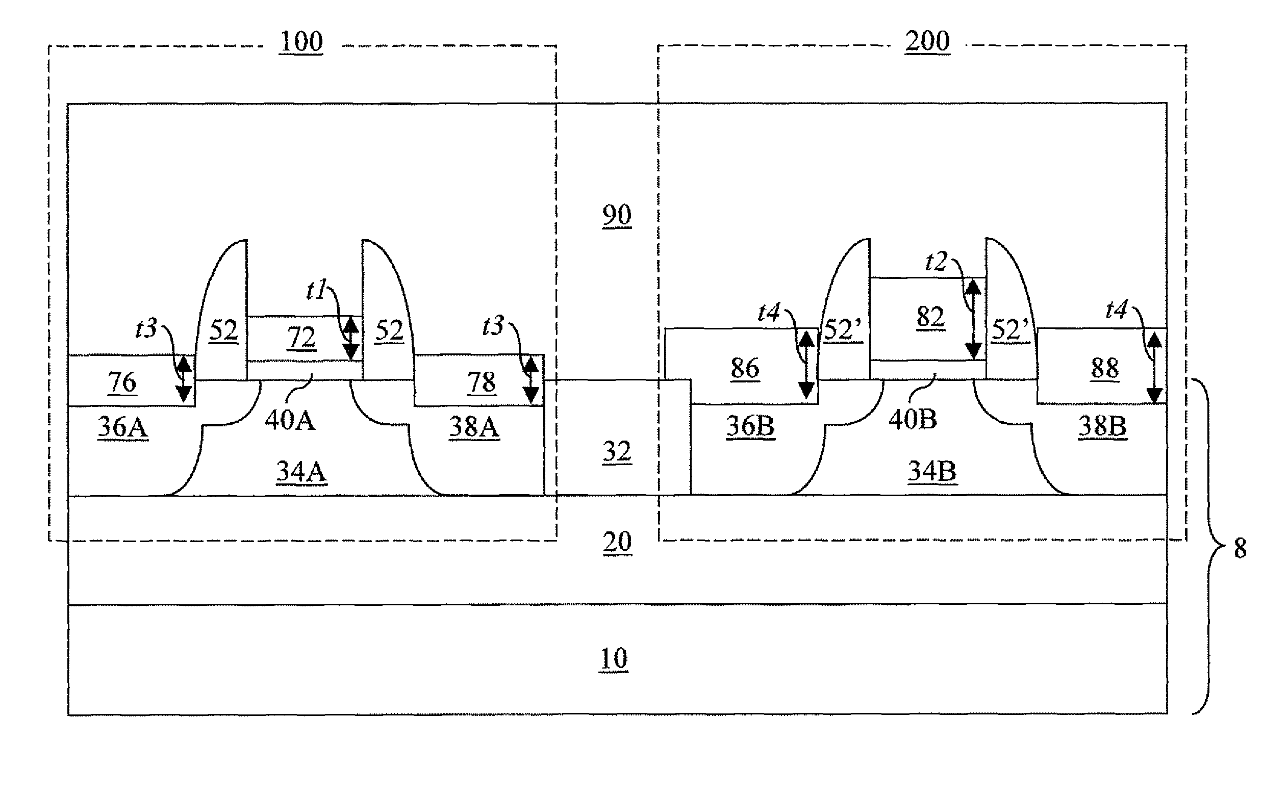
[0060]As stated above, the present invention relates to a complementary metal oxide semiconductor (CMOS) transistor having a metal silicide electrode and a metal silicide-germanide alloy electrode, and methods of manufacturing the same, which are now described in detail with accompanying figures. It is noted that like and corresponding elements are referred to by like reference numerals.

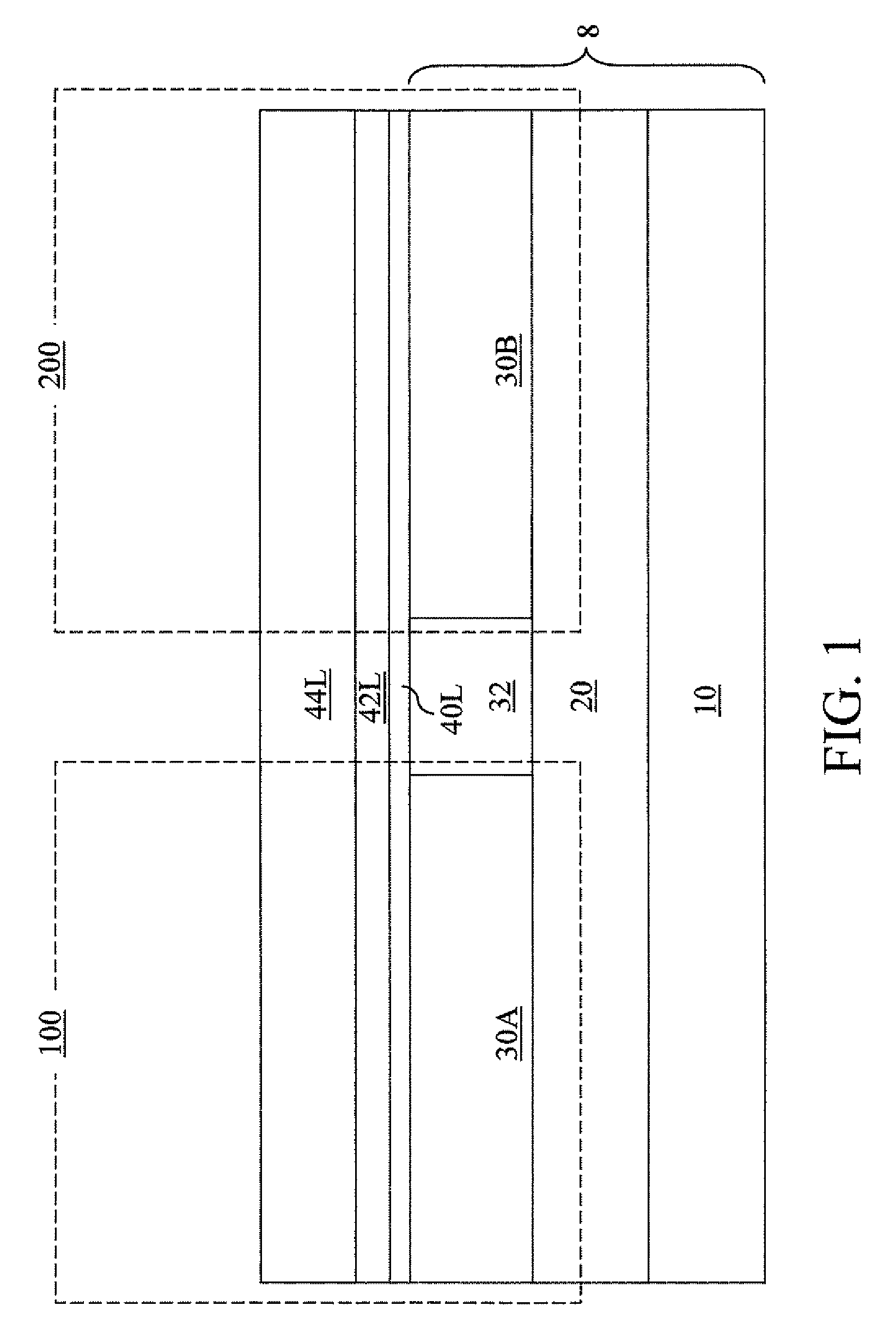
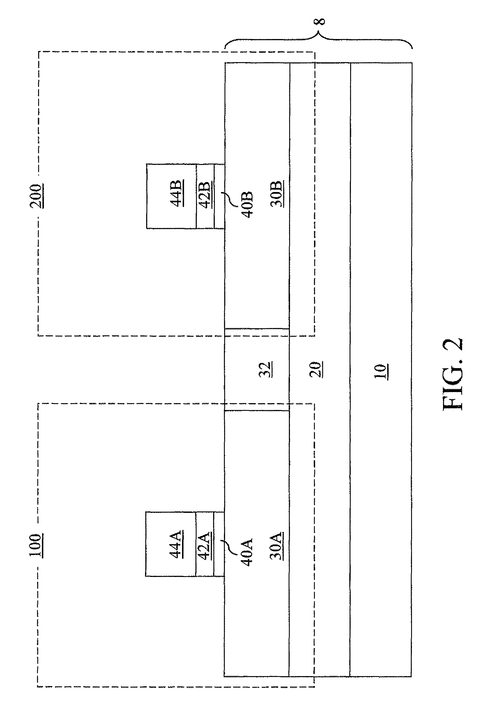
[0061]Referring to FIG. 1, an exemplary semiconductor structure according to the present invention comprises a semiconductor substrate 8 containing a handle substrate 10, a buried insulator layer 20, and a top semiconductor layer including a first semiconductor portion 30A, a second semiconductor portion 30B, and a shallow trench isolation structure 32. The first semiconductor portion 30A and the second semiconductor portion 30B comprise a semiconductor material, which may be selected from, but is not limited to, silicon, germanium, silicon-germanium alloy, silicon carbon alloy, silicon-germanium-car...


PUM

PropertyMeasurementUnit
temperatureaaaaaaaaaa
temperaturesaaaaaaaaaa
work functionaaaaaaaaaa

Abstract

A p-type field effect transistor (PFET) and an n-type field effect transistor (NFET) are formed by patterning of a gate dielectric layer, a thin silicon layer, and a silicon-germanium alloy layer. After formation of the source / drain regions and gate spacers, silicon germanium alloy portions are removed from gate stacks. A dielectric layer is formed and patterned to cover an NFET gate electrode, while exposing a thin silicon portion for a PFET. Germanium is selectively deposited on semiconductor surfaces including the exposed silicon portion. The dielectric layer is removed and a metal layer is deposited and reacted with underlying semiconductor material to form a metal silicide for a gate electrode of the NFET, while forming a metal silicide-germanide alloy for a gate electrode of the PFET.

Description

FIELD OF THE INVENTION[0001]The present invention relates to a semiconductor structure, and more particularly to a complementary metal oxide semiconductor (CMOS) transistor having a metal silicide electrode and a metal silicide-germanide alloy electrode, and methods of manufacturing the same.BACKGROUND OF THE INVENTION[0002]A field effect transistor having a metal gate electrode has enhanced performance over a comparable field effect transistor having a polysilicon electrode due to higher conductivity of the gate electrode, and consequently, a reduced signal delay in the operation of the transistor. Further, the polysilicon depletion effect is eliminated by the metal gate electrode, which allows the gate dielectric to be electrically thinner. In addition, boron dopant diffusion into the channel region is eliminated in the case of p-type field effect transistors. While such benefits of the metal gate electrode are known in the art, integration of metal gate electrodes has proven to b...

Claims


Application Information

Patent Timeline
Patent Type & Authority Patents(United States)
IPC IPC(8): H01L21/8238H01L27/092
CPCH01L21/28052H01L21/28518H01L21/823835H01L21/823842H01L29/4933H01L29/517H01L29/665H01L29/66545H01L21/82385Y10S438/933
Inventor CABRAL, JR., CYRILCHU, JACK O.KIM, YOUNG-HEE
Owner IBM CORP
Why Eureka
Try Eureka