Sequential deposition/anneal film densification method

Active Publication Date: 2010-09-07
NOVELLUS SYSTEMS
View PDF219 Cites 436 Cited by
  • Summary
  • Abstract
  • Description
  • Claims
  • Application Information

AI Technical Summary

Benefits of technology

[0008]The present invention addresses this need by providing a multi-step method of forming a densified silicon oxide-based dielectric film. First, a thin layer of silicon oxide-based dielectric is thermally deposited. Then, the dielectric film is densified by an annealing process that removes water from the deposited layer. The deposition and anne

Problems solved by technology

Non-uniformity of the etch causes overhang features which contribute to problems including the formation of voids during high aspect ratio gap fill.
In general, the layer is sufficiently thin to not prevent substantially complete penetration of the annealing agent into the layer and mi

Method used


Image

  • Sequential deposition/anneal film densification method
  • Sequential deposition/anneal film densification method
  • Sequential deposition/anneal film densification method

Examples


##p embodiment

RVD / HDP Embodiment

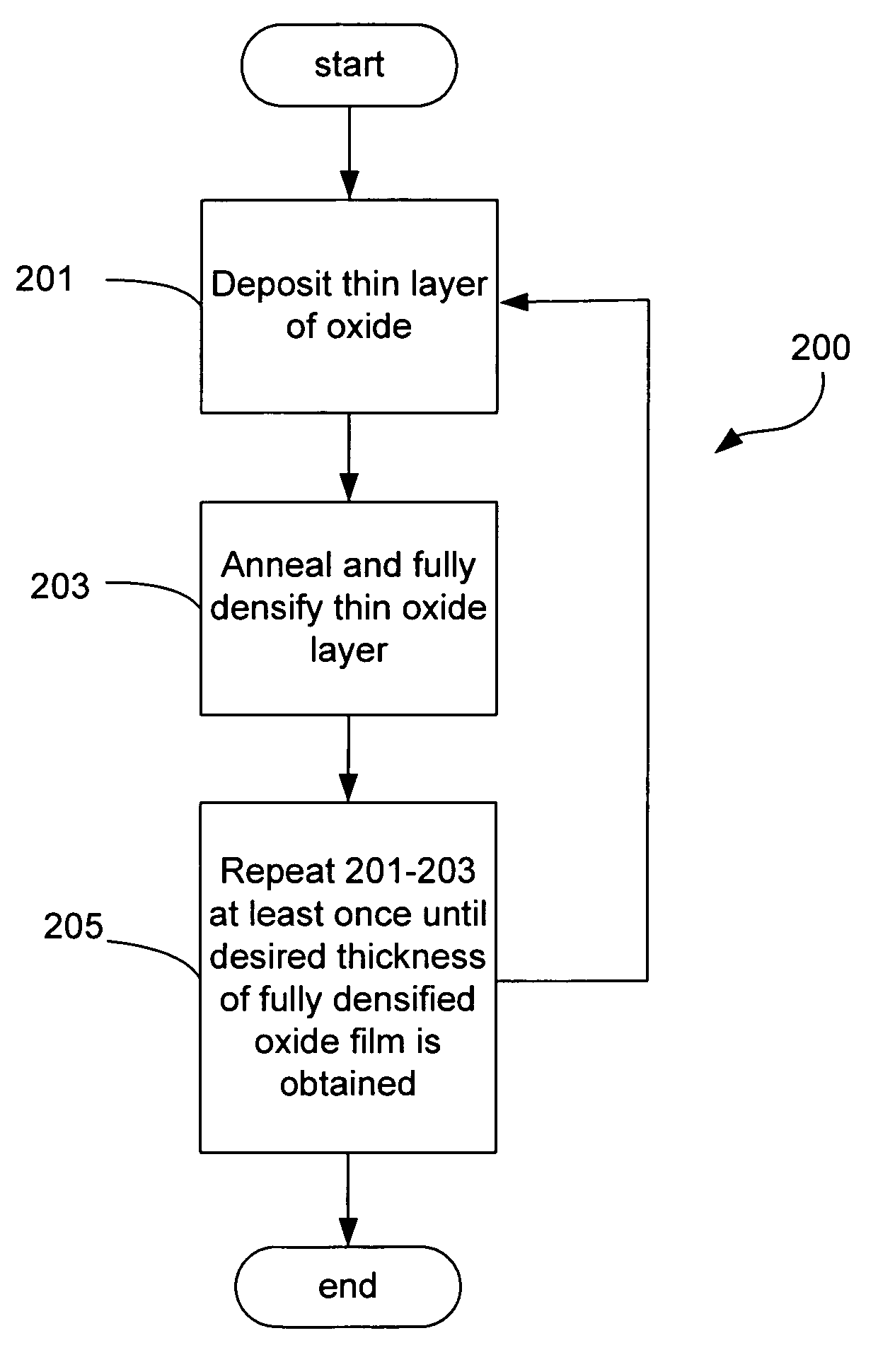
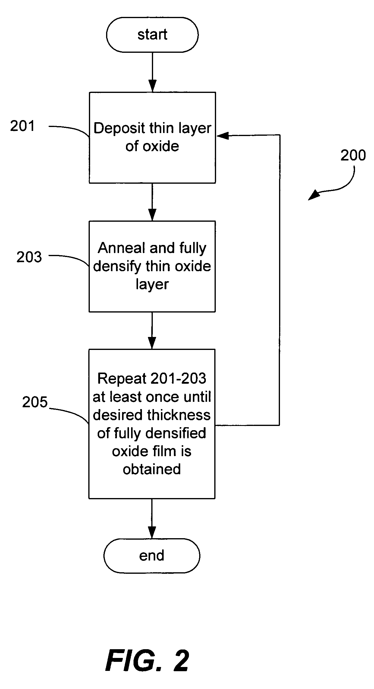
[0038]A preferred annealing process is high density plasma (HDP)-based. A high density plasma in an oxidizing environment can fully and uniformly densify thin dielectric films at low temperatures. This technique has the advantage of annealing while staying within the thermal budget constraints of temperature sensitive dielectric formation applications, e.g., PMD.

[0039]Generally, a RVD method involves sequentially depositing a plurality of atomic-scale films on a substrate surface by sequentially exposing and removing reactants to and from the substrate surface. An exemplary case of RVD using reactant gases A and B will now be used to illustrate principle operations of a RVD process in accordance with the present invention. First, gas A is injected into a chamber and the molecules of gas A are chemically or physically adsorbed to the surface of a substrate, thereby forming a “saturated layer” of A. Formation of a saturated layer is self-limiting in nature and repres...

example

[0082]The following example provides details relating to performance advantages of the present invention. It should be understood the following is representative only, and that the invention is not limited by the detail set forth in this example.

[0083]Annealing Efficiency

[0084]FIG. 7 shows the effect of film thickness on the efficiency of the densification (annealing) process. SiO2 films were deposited by RVD using a silicon precursor partial pressure below 10 Torr and a temperature of 230° C. Films were annealed by RTP at the temperatures indicated for at least 5 minutes at ambient pressure in a mixture of 30% steam and 70% N2. The films' wet etch rate, which is a measure of film density, was measured at the top and at the bottom of the stack. For the 5000 Å films, the difference is in the order of 40%, while for films 2000 Å thick the wet etch rate measurements were within 12% at temperatures above 700° C. This result indicates that the thinner films were more efficiently and unif...


PUM


Abstract

A silicon dioxide-based dielectric layer is formed on a substrate surface by a sequential deposition/anneal technique. The deposited layer thickness is insufficient to prevent substantially complete penetration of annealing process agents into the layer and migration of water out of the layer. The dielectric layer is then annealed, ideally at a moderate temperature, to remove water and thereby fully densify the film. The deposition and anneal processes are then repeated until a desired dielectric film thickness is achieved.

Description

CROSS-REFERENCE TO RELATED APPLICATIONS[0001]This application is a continuation-in-part of U.S. patent application Ser. No. 10 / 975,028 filed Oct. 26, 2004 now U.S. Pat. No. 7,148,155, titled SEQUENTIAL DEPOSITION / ANNEAL FILM DENSIFICATION METHOD, incorporated herein by reference in its entirety for all purposes.BACKGROUND OF THE INVENTION[0002]The present invention relates to the formation of dielectric films, in particular to the formation of dense dielectric films in high aspect ratio features on semiconductor substrates.[0003]It is often necessary in semiconductor processing to fill a high aspect ratio gap with insulating material. One example of a high aspect ratio trench encountered in semi-conductor processing is in the formation of shallow trench isolation (STI). As device dimensions shrink and thermal budgets are reduced, void-free filling of high aspect ratio spaces (AR>3.0:1) becomes increasingly difficult due to limitations of existing deposition processes. The deposit...

Claims


Application Information

Patent Timeline
IPC IPC(8): H01L21/31H01L21/469
CPCH01L21/02164H01L21/0228H01L21/02312H01L21/02315H01L21/02345H01L21/02348H01L21/02351H01L21/02354H01L21/76224
Inventor TARAFDAR, RAIHAN M.PAPASOULIOTIS, GEORGE D.RULKENS, RONHAUSMANN, DENNIS M.TOBIN, JEFFTIPTON, ADRIANNE K.NIE, BUNSEN
Owner NOVELLUS SYSTEMS
Why Eureka
Try Eureka