Negative electrode for nonaqueous secondary battery, process of producing the negative electrode, and nonaqueous secondary battery
a secondary battery and negative electrode technology, applied in secondary cell servicing/maintenance, cell components, electrochemical generators, etc., can solve the problems of difficult to meet the increasing demands in the near future, not yet been put to practical use, and the power consumption of these devices has shown a remarkable increase. , to achieve the effect of improving the electrical conductivity of the negative electrode, improving the electron conductivity, and improving the electrical conductivity
- Summary
- Abstract
- Description
- Claims
- Application Information
AI Technical Summary
Benefits of technology
Problems solved by technology
Method used
Image
Examples
example 1-1
(1) Preparation of Active Material Particles
[0101]A molten metal at 1400° C. containing 90% of silicon and 10% of nickel was cast into a copper-made mold and quenched to obtain an ingot of a silicon-nickel alloy. The ingot was pulverized and sieved to obtain silicon-nickel alloy particles having particle sizes of 0.1 to 10 μm. The silicon-nickel alloy particles and nickel particles (particle size: 30 μm) were blended at a rate of 80% 20% and mixed and pulverized simultaneously in an attritor to obtain uniformly mixed particles of silicon-nickel particles and nickel. The mixed particles had the maximum particle size of 1 μm and a D50 value of 0.8 μm.
(2) Preparation of Slurry
[0102]A slurry having the following composition was prepared.
[0103]
Mixed particles obtained in (1) above16%Acetylene black (particle size: 0.1 μm)2%Binder (polyvinylidene fluoride)2%Diluting solvent (N-methylpyrrolidone)80%
(3) Formation of Active Material Layer
[0104]The above prepared slurry was applied to a 35 μm...
examples 1-2 to 1-4
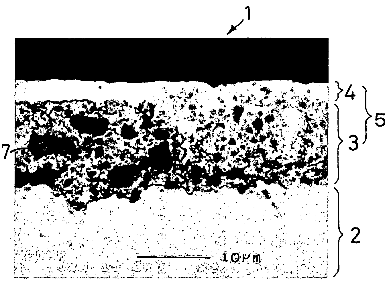
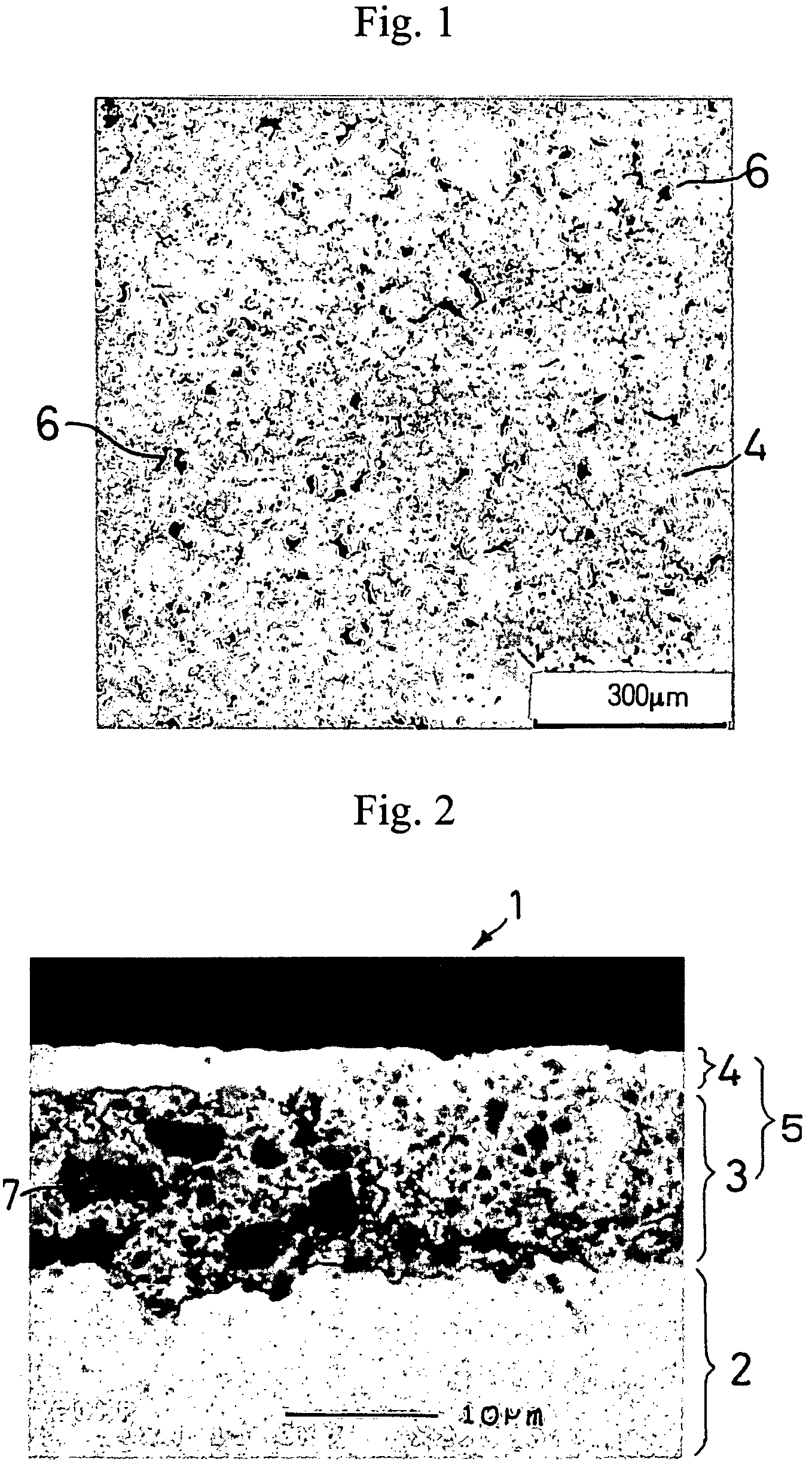
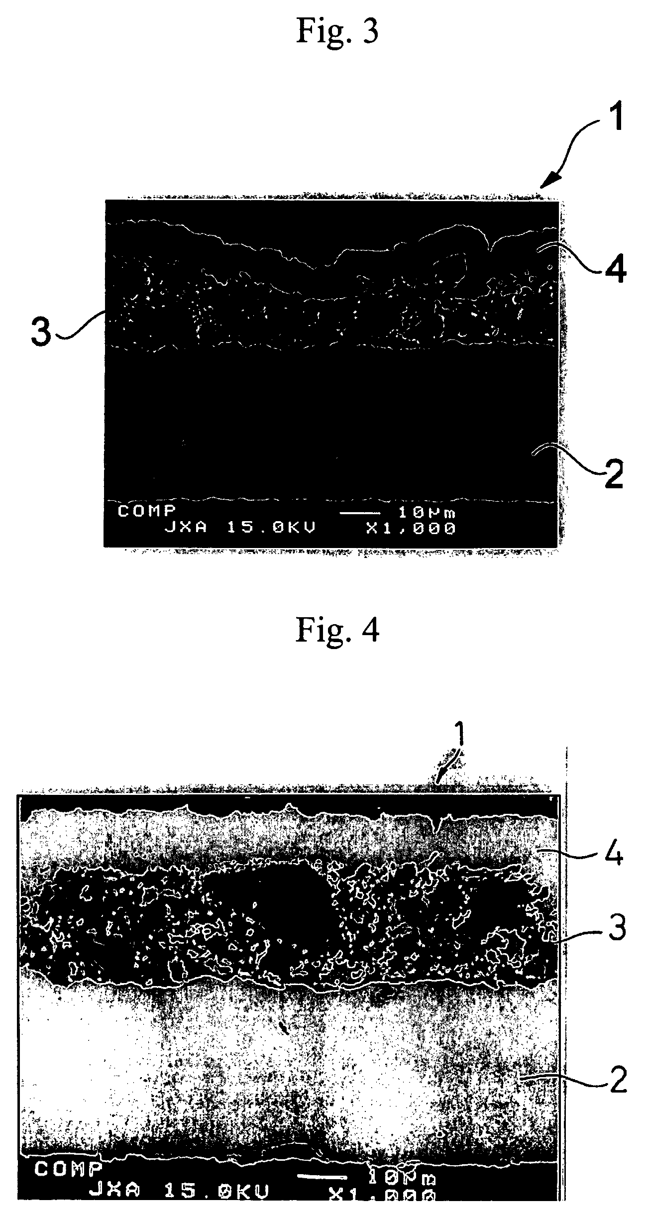
[0108]A negative electrode was produced in the same manner as in Example 1-1, except for using the active material particles shown in Table 1-1 below. The same electron microscopic observation as in Example 1-1 revealed presence of micropores in the resulting negative electrode.
example 1-5
[0109]A 35 μm thick copper foil was plated with nickel to a deposit thickness of 2 μm to prepare a current collector. An active material layer and a surface coating layer were formed on the nickel layer in the same manner as in Example 1-1, except for using the active material particles shown in Table 1-1 in the active material layer. The same electron microscopic observation as in Example 1-1 revealed presence of micropores in the resulting negative electrode.
PUM
| Property | Measurement | Unit |
|---|---|---|
| surface roughness | aaaaa | aaaaa |
| optical transmittance | aaaaa | aaaaa |
| particle size | aaaaa | aaaaa |
Abstract
Description
Claims
Application Information


