Packaging substrate and method for fabricating the same

a technology of packaging substrates and substrates, which is applied in the manufacture of printed circuits, printed circuit aspects, basic electric elements, etc., can solve the problems of difficult thickness of flip-chip solder pads, solder ball pads, etc., to prevent copper migration, facilitate the wire bonding process, and prevent short circuits

Active Publication Date: 2010-10-12
UNIMICRON TECH CORP
View PDF6 Cites 6 Cited by
  • Summary
  • Abstract
  • Description
  • Claims
  • Application Information

AI Technical Summary

Benefits of technology

[0014]To overcome the above drawbacks, an objective of the present invention is to provide a packaging substrate and a method for fabricating the same such that integrated wire bonding and flip-chip packages can meet requirements for fine-pitch applications.
[0015]Another objective of the present invention is to provide a packaging substrate and a method for fabricating the same so as to improve the electrical connection reliability.
[0025]Compared with the conventional electroplated Ni / Au layer, the electroless Ni / Pd / Au layer of the present invention is helpful to prevent copper migration so as to prevent a short circuit. Meanwhile, the electroless Ni / Pd / Au layer formed by electroless plating has a thickness tolerance capable of meeting evenness requirements for fine pitch applications. Further, the electroless Ni / Pd / Au layer applied to the flip-chip solder pads or solder ball pads and even the first and second bumps can prevent detachment of solder bumps or solder balls. In addition, the electroless Ni / Pd / Au layer formed on the wire bonding pads can facilitate the wire bonding process.
[0026]Furthermore, instead of using the conventional screen printing, the present invention forms the first bumps by electroplating. Thus, the average size and height tolerance are easy to control so as to overcome the conventional problems of underfilling difficulty, joint bridge and uneven joint stresses caused by poor coplanarity of the bumps. The recess portions of the first bumps further alleviate stresses between the semiconductor chips and the packaging substrate.
[0027]Therefore, the packaging substrate of the present invention improves the electrical connection reliability and makes integrated wire bonding and flip-chip packages capable of meeting requirements for fine pitch applications.

Problems solved by technology

Firstly, with the surface treatment layer 12 being made of a solder material (SnPb, SnAg, SnCu, SnAgCu), immersion tin or OSP, it is difficult to prevent copper migration that may otherwise cause a short circuit.
Further, along with the continuous increase of the thickness of an IMC (intermetallic compound) layer formed at the Sn—Cu interface, the thickness of the flip-chip solder pads 101 and the solder ball pads 103 continuously decreases, thereby adversely affecting the joint reliability.
Secondly, the surface treatment layer 12 which is an electroplated Ni / Au layer does not have fine-pitch applications for failure to meet evenness requirements for the fine-pitch applications.
Therefore, the surface treatment layer cannot be applied to hand-held products.
If the surface treatment layer is formed on the wire bonding pads 102, there will be poor attachment between the Au layer and the conductive wires 16 because the Au layer formed by electroless plating is quite thin and structurally weak.
Fourthly, if the solder bumps 13 are formed by screen printing, a fine pitch cannot be achieved because the average size and height tolerance of the solder bumps 13 cannot be controlled well enough.
If the solder bumps 13 are formed on the flip-chip solder pads 101 and the average size or height of the solder bumps 13 is small, an underfill process can be adversely affected.
In addition, given large height tolerance of the solder bumps 13, chips can easily be damaged due to uneven joint stresses caused by poor coplanarity.
Therefore, the semiconductor industry is in dire need of a solution to overcome the above drawbacks.

Method used


Image

  • Packaging substrate and method for fabricating the same
  • Packaging substrate and method for fabricating the same
  • Packaging substrate and method for fabricating the same

Examples


first embodiment

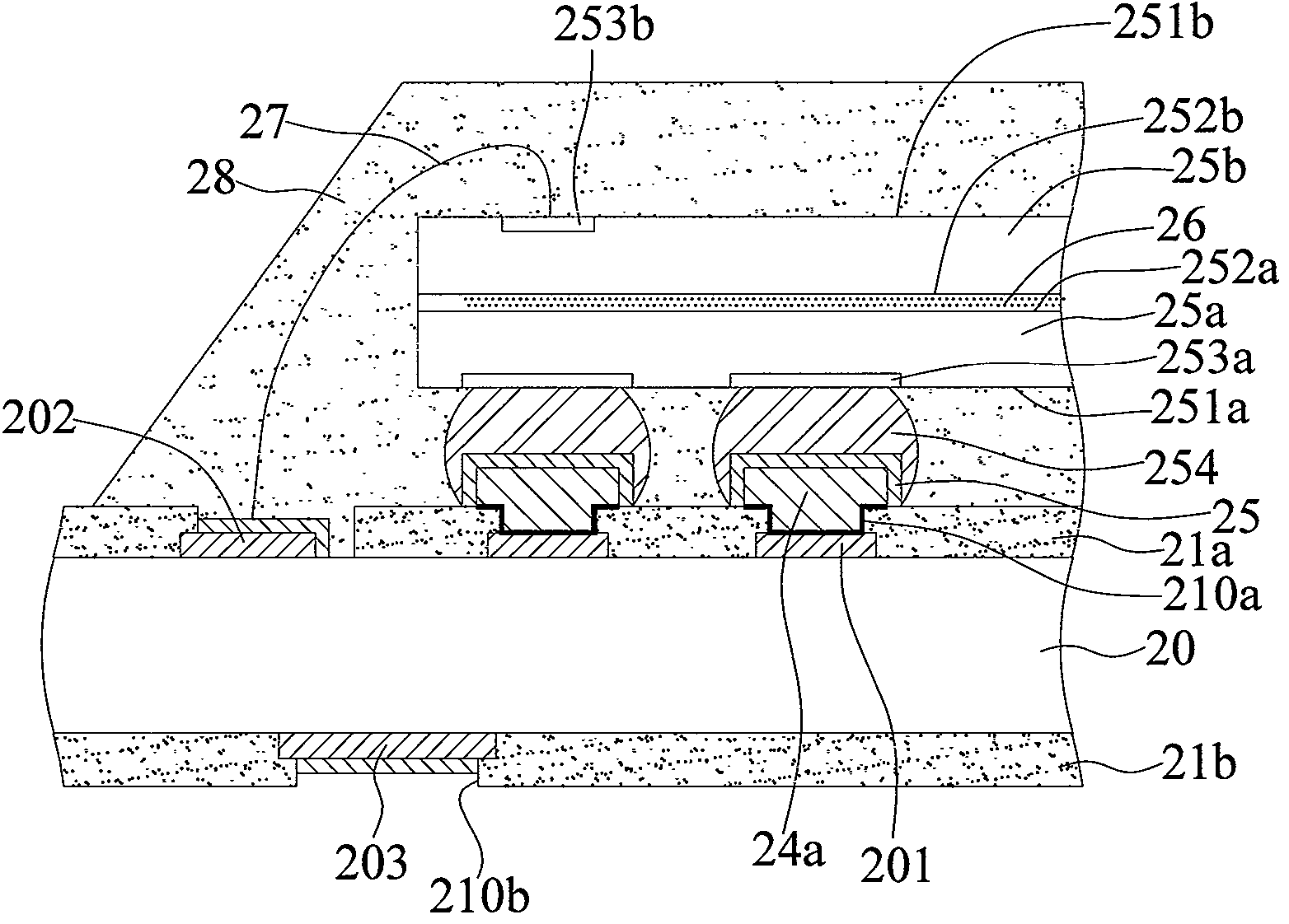
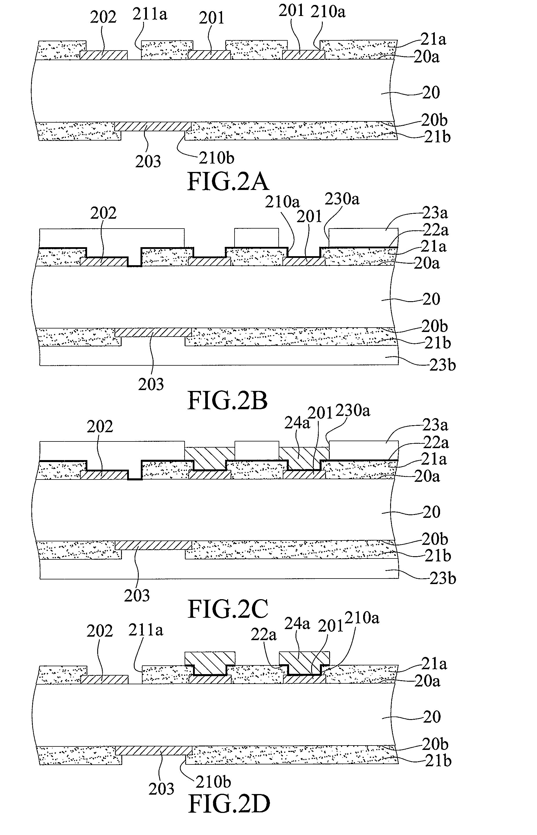
[0033]FIGS. 2A to 2E are sectional views showing a packaging substrate and a method for fabricating the same according to a first embodiment of the present invention.

[0034]As shown in FIG. 2A, a substrate body 20 having a first surface 20a and an opposing second surface 20b is provided. A plurality of flip-chip solder pads 201 and wire bonding pads 202 are formed on the first surface 20a. A plurality of solder ball pads 203 are formed on the second surface 20b. A first solder mask layer 21a and a second solder mask layer 21b are formed on the first surface 20a and the second surface 20b, respectively. A plurality of first openings 210a and second openings 211a are formed in the first solder mask layer 21a so as to allow the flip-chip solder pads 201 to be exposed from the first openings 210a and allow the wire bonding pads 202 as well as the first surface 20a around the wire bonding pads 202 to be exposed from the second openings 211a. A plurality of third openings 210b are formed i...

second embodiment

[0045]FIGS. 3A to 3D are cross-sectional views of a packaging substrate and a method for fabricating the same according to a second embodiment of the present invention. The second embodiment differs from the first embodiment in that, in the second embodiment, a plurality of second bumps are formed on the solder ball pads.

[0046]As shown in FIG. 3A, a structure as shown in FIG. 2A is provided. Then, a first conductive layer 22a is formed on the first solder mask layer 21a, the flip-chip solder pads 201, the wire bonding pads 202 and the first surface 20a of the substrate body 20, wherein the first conductive layer 22a comprises a palladium material. A first resist layer 23a is formed on the first conductive layer 22a. A plurality of first openings 230a are formed in the first resist layer 23a to expose the first conductive layer 22a on the flip-chip solder pads 201 and around the flip-chip solder pads 201. A second conductive layer 22b is formed on the second solder mask layer 21b and...


PUM

PropertyMeasurementUnit
widthaaaaaaaaaa
diameteraaaaaaaaaa
conductiveaaaaaaaaaa

Abstract

A packaging substrate and a method for fabricating the same are proposed, including: providing a substrate body having a first surface and an opposing second surface, wherein the first surface has a plurality of flip-chip solder pads and wire bonding pads and the second surface has a plurality of solder ball pads; forming a first and a second solder mask layers on the first and second surfaces respectively and forming openings in the first and second solder mask layers to expose the flip-chip solder pads, the wire bonding pads and the solder ball pads; forming first bumps on the flip-chip solder pads; and forming an electroless Ni / Pd / Au layer on the first bumps and the wire bonding pads by electroless plating, wherein the electroless Ni / Pd / Au layer has a thickness tolerance capable of meeting evenness requirements for fine pitch applications.

Description

BACKGROUND OF THE INVENTION[0001]1. Field of the Invention[0002]The present invention relates generally to packaging substrates and methods for fabricating the same, and more particularly, to a packaging substrate with a reinforced electrical connection structure and a method for fabricating the same.[0003]2. Description of Related Art[0004]Along with the rapid development of electronic industries, electronic products are becoming lighter, thinner, shorter and smaller. There is a trend towards high-performance, high-functionality, and high-speed electronic products. In a conventional semiconductor package structure, an inactive surface of a semiconductor chip is attached to a packaging substrate and an active surface of the semiconductor chip is electrically connected to the packaging substrate through bonding wires. Alternatively, the active surface of the semiconductor chip can be electrically connected to the packaging substrate by flip-chip technique. Further, a plurality of sol...

Claims


Application Information

Patent Timeline
Patent Type & Authority Patents(United States)
IPC IPC(8): H01L23/48H01L23/52H01L29/40
CPCH01L23/49816H01L25/0657H05K3/243H01L23/49866H01L24/45H01L24/16H01L24/48H01L2224/16H01L2224/48091H01L2224/48227H01L2225/0651H01L2225/06517H01L2924/01046H01L2924/01078H01L2924/01079H05K1/111H05K3/3436H05K2201/0367H05K2201/0391H05K2203/049H05K2203/054H01L2924/00014H01L2224/45144H01L2924/01327H01L2924/01055H01L2224/05599H01L2224/05571H01L2224/05573H01L2224/16225H01L2224/32145H01L2224/73265H01L2924/181H01L2924/00012H01L2924/00
Inventor HSU, SHIH-PING
Owner UNIMICRON TECH CORP
Why Eureka
Try Eureka