Lateral field effect transistor and its fabrication comprising a spacer layer above and below the channel layer

a technology of lateral field effect transistor and spacer layer, which is applied in the direction of transistors, basic electric elements, electric devices, etc., can solve the problems of reducing gate length, increasing power and operation frequency, and affecting the operation speed of the transistor, so as to achieve the effect of increasing the operation speed

Active Publication Date: 2010-11-16
CREE SWEDEN
View PDF7 Cites 0 Cited by
  • Summary
  • Abstract
  • Description
  • Claims
  • Application Information

AI Technical Summary

Benefits of technology

[0012]The object of the present invention is to provide a lateral field effect transistor of the type defined in the introduction, which has an increased operation speed, which may be operated at a higher power, which is more thermally stable than prior art transistors and which eliminates the above-mentioned drawbacks associated with prior art transistors.
[0018]The utilization of a spacer layer between the channel layer and the highly doped second-conductivity-type base layer improves the performance of the transistor since the highly doped second-conductivity-type base layer is a parasitic gate.
[0020]According to another preferred embodiment of the invention the gate electrode is recessed into the spacer layer located between the gate electrode and the channel layer so as to control the threshold voltage. The closer the gate electrode to the channel layer the better the Schottky contact.
[0025]Since the channel layer is highly doped, the carrier mobility in the channel layer is suppressed due to the scattering of carriers by the impurities. However the mobility of carriers in the highly doped channel layer has a very low temperature dependency at high temperatures. This provides for more thermally stable components suitable for use in high temperature applications and high power applications in which there is always considerable heat dissipation.
[0028]According to a preferred embodiment of the invention an insulation layer is arranged between the gate electrode and the spacer layer so as to provide better high temperature capabilities.
[0029]According to another preferred embodiment of the invention the highly doped second-conductivity-type base layer totally overlaps the gate electrode. According to a further preferred embodiment of the invention the highly doped p-type base layer may protect the entire region between the source and the drain-side edge of the gate.

Problems solved by technology

Shorter gates therefore result in higher power and higher operation frequency.
However, undesirable short-channel effects become significant as the gate length is decreased.
Furthermore, the p-n-junction so created can block higher voltages than a Schottky barrier, resulting in an increase of the possible power.
Such a structure, while improving the performance of a transistor is however prone to carrier trapping in the presence of a dielectric, i.e. carriers are held by traps (i.e. electrically active defects at the interface between the dielectric and the semiconductor) for a while before they escape back into their band of origin.
Trapping decreases the current flowing through the channel layer and consequently affects the performance of the component.
It has also been found that surface-state-related instabilities occur when a high drain bias is applied.

Method used


Image

  • Lateral field effect transistor and its fabrication comprising a spacer layer above and below the channel layer
  • Lateral field effect transistor and its fabrication comprising a spacer layer above and below the channel layer
  • Lateral field effect transistor and its fabrication comprising a spacer layer above and below the channel layer

Examples


Embodiment Construction

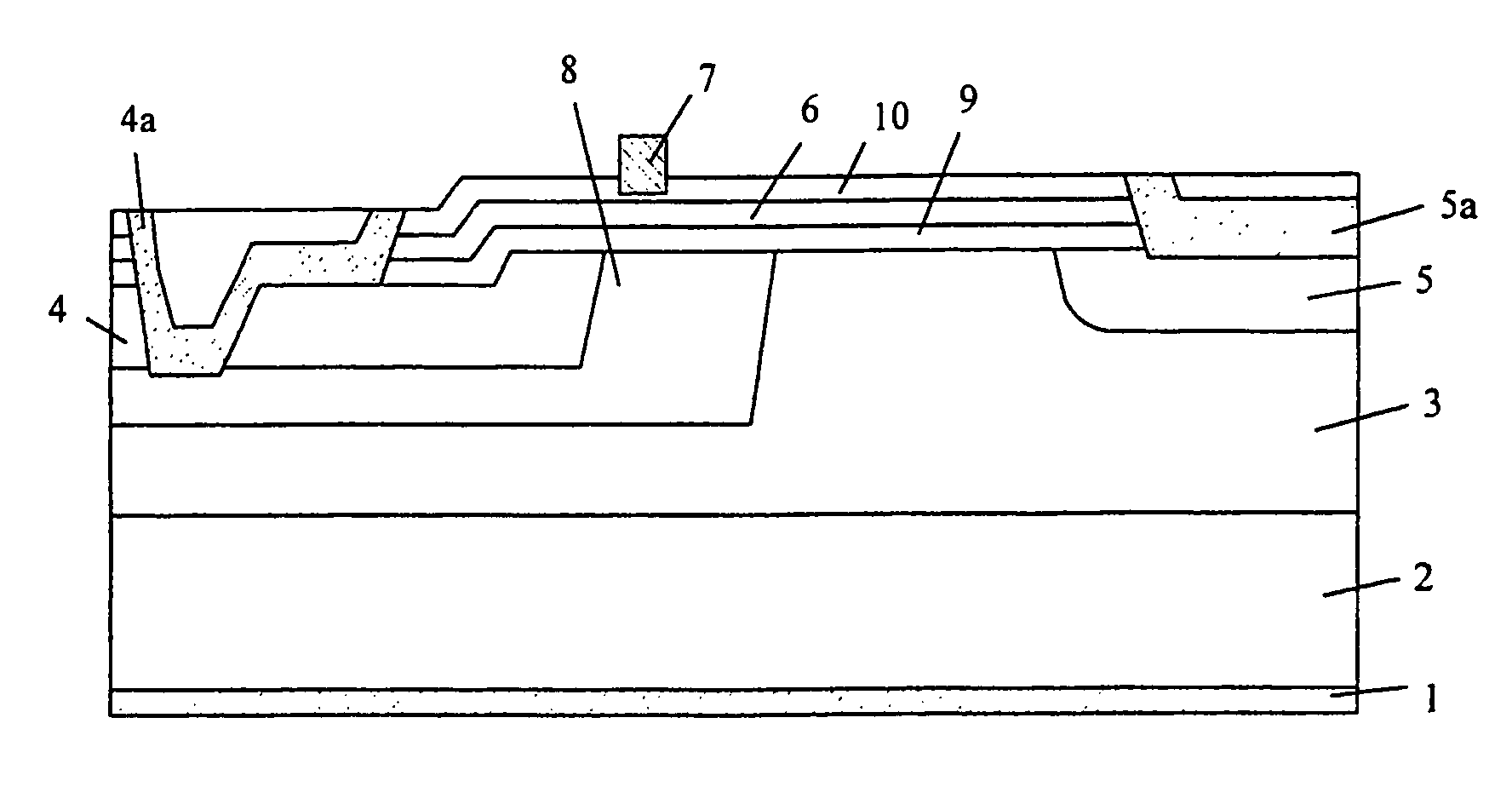
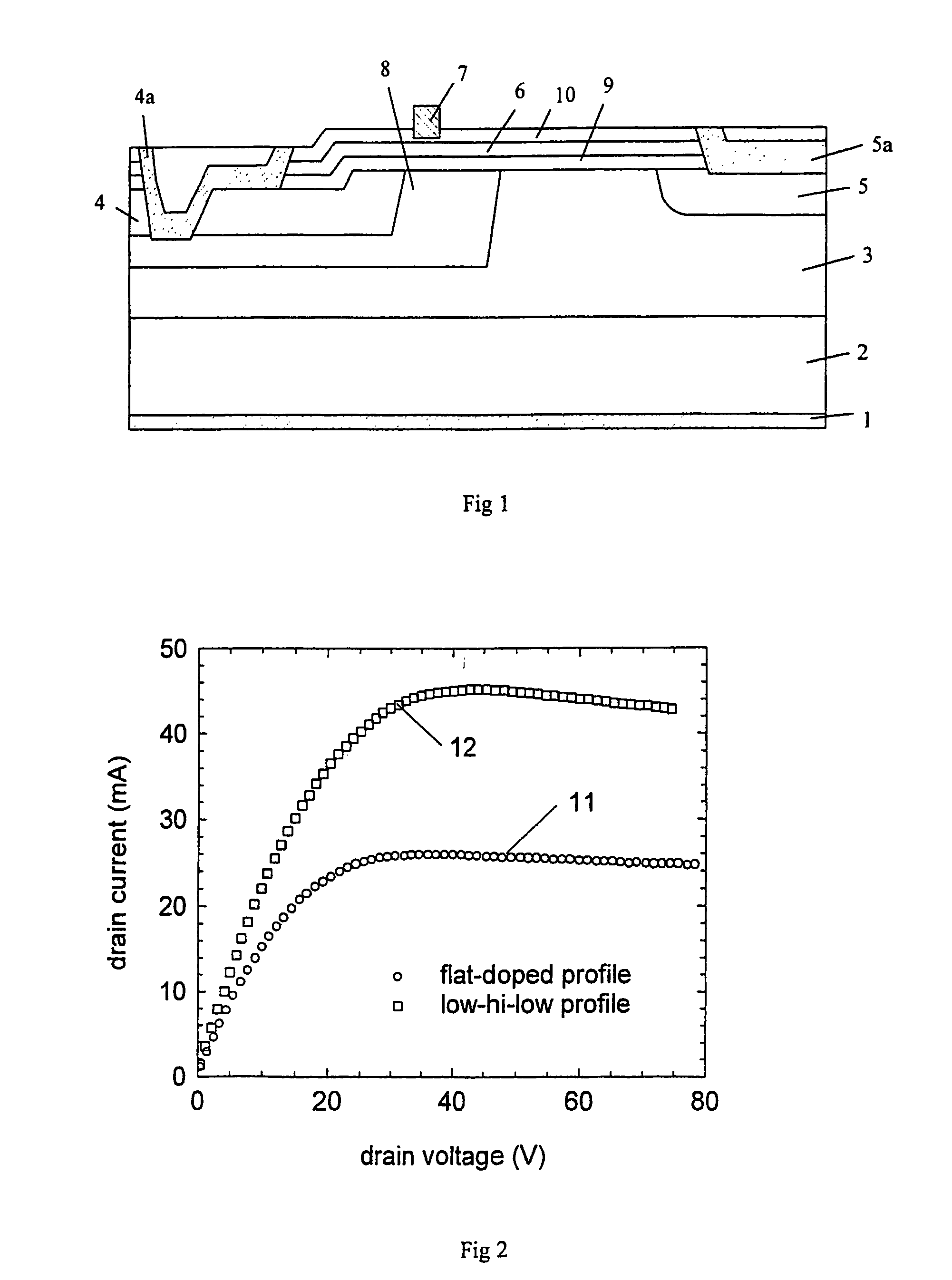
[0042]The following example relates to a SiC field effect transistor however the present invention concerns field effect transistors comprising any semiconductor material. Since the mobility of free electrons in SiC is considerably higher than the mobility of valence-band holes, all microwave SiC transistors are of the n-p-n type. An n-p-n transistor is therefore given by way of example.

[0043]The transistor shown in FIG. 1 comprises layers of SiC on top of a back-side metallization layer 1. The transistor comprises a semi-insulating substrate layer 2 and a p-type buffer layer 3 which minimizes the effect of the deep centres present in the semi-insulating substrate on carrier transport. The doping level of the buffer layer should be low to keep high frequency losses at a low level.

[0044]The transistor further comprises a highly doped source region layer 4 and a highly doped drain region layer 5 which are laterally spaced. A source contact 4a and a drain contact 5a are arranged on the...


PUM


Abstract

A lateral field effect transistor for high switching frequencies having a source region layer (4) and a drain region layer (5) laterally spaced and of highly doped first conductivity type, a first-conductivity-type channel layer (6) of lower doping concentration extending laterally and interconnecting the source region layer (4) and the drain region layer (5). The transistor has a gate electrode (7) arranged to control the properties of the channel layer (6), and a second-conductivity-type base layer (8) arranged under the channel layer (6) at least partially overlapping the gate electrode (7) and at a lateral distance to the drain region layer (5), the highly doped second-conductivity-type base layer (8) being shorted to the source region layer (4). The transistor also has at least one of the following: a) a spacer layer (10) having semiconductor material adjacent to the channel layer (6) and located between the channel layer (6) and gate electrode (7), at least in the vicinity of the gate electrode (7), and / or b) a spacer layer (9) having semiconductor material adjacent to the channel layer (6) and located between the channel layer (6) and the second-conductivity-type base layer (8).

Description

TECHNICAL FIELD OF THE INVENTION AND PRIOR ART[0001]The present invention relates to a lateral field effect transistor, such as a JFET, MESFET, MISFET or MOSFET, for high switching frequencies (above 1 MHz and preferably above 1 GHz). The transistor comprises a source region layer and a drain region layer laterally spaced and of highly doped n-type, an n-type channel layer of lower doping concentration extending laterally and interconnecting the source region layer and the drain region layer for conducting a current between these layers in the on-state of the transistor.[0002]The transistor also comprises a gate electrode arranged to control the properties of the channel layer to be conducting or blocking by varying the potential applied to the gate electrode. Furthermore the transistor comprises a highly doped p-type base layer arranged under the channel layer at least partially overlapping the gate electrode and being at a lateral distance to the drain region layer, said highly do...

Claims


Application Information

Patent Timeline
Patent Type & Authority Patents(United States)
IPC IPC(8): H01L29/94
CPCH01L21/0465H01L29/1029H01L29/1058H01L29/66068H01L29/802H01L29/808H01L29/812H01L29/1608H01L29/2003
Inventor HARRIS, CHRISTOPHERKONSTANTINOV, ANDREI
Owner CREE SWEDEN
Why Eureka
Try Eureka