

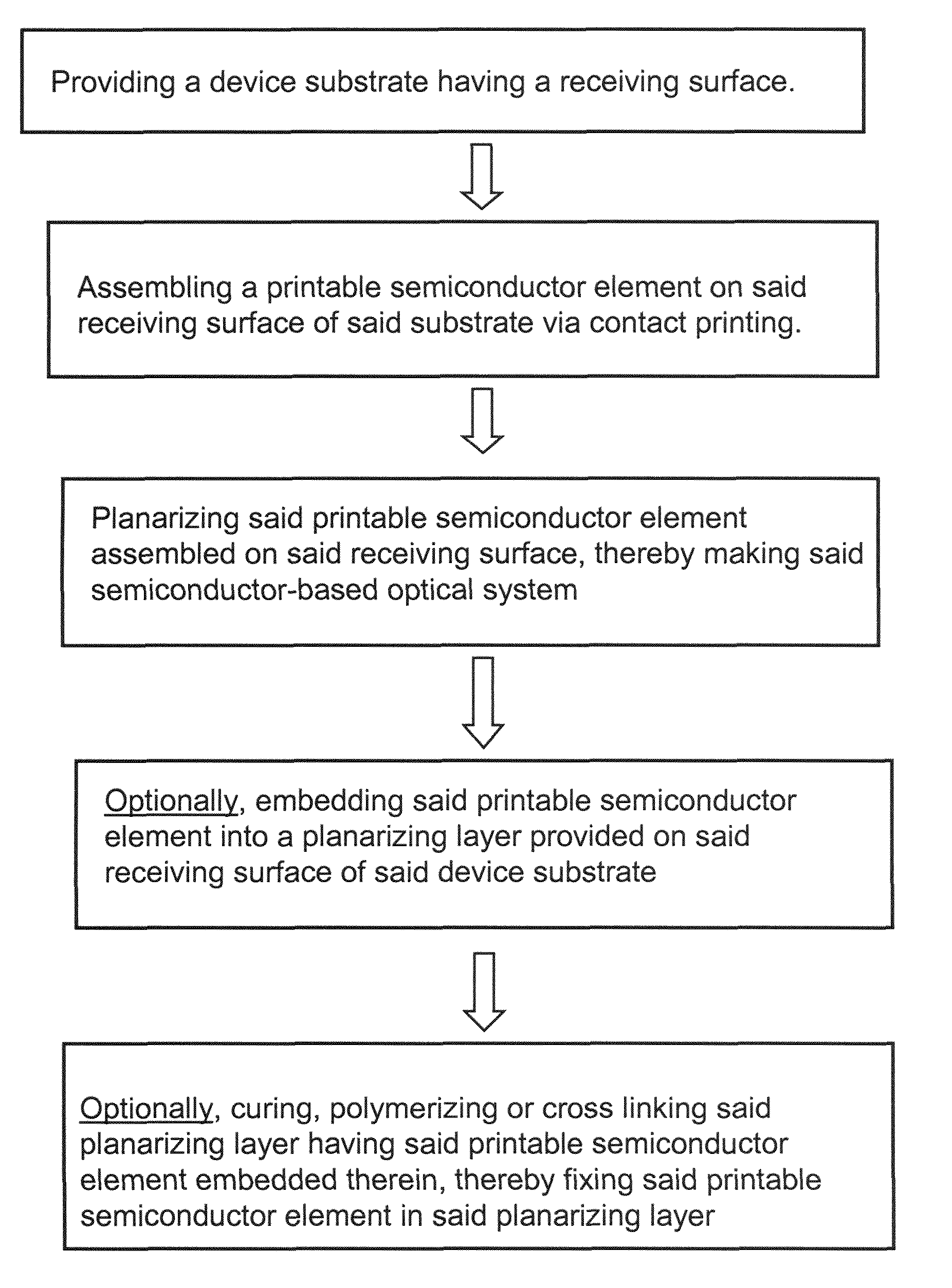
Optical systems fabricated by printing-based assembly
a technology of optical systems and assembly, applied in the direction of sustainable manufacturing/processing, semiconductor lasers, final product manufacturing, etc., can solve the problems of inability to exhibit electronic properties comparable to conventional single crystalline silicon based electronic devices, inability to withstand bending or deformation, etc., to achieve a wide range of mechanical properties, improve the mechanical stability and ruggedness, and minimize the strain on these elements during bending or deformation.
- Summary
- Abstract
- Description
- Claims
- Application Information
AI Technical Summary
Benefits of technology
Problems solved by technology
Method used
Image

Examples
example 1
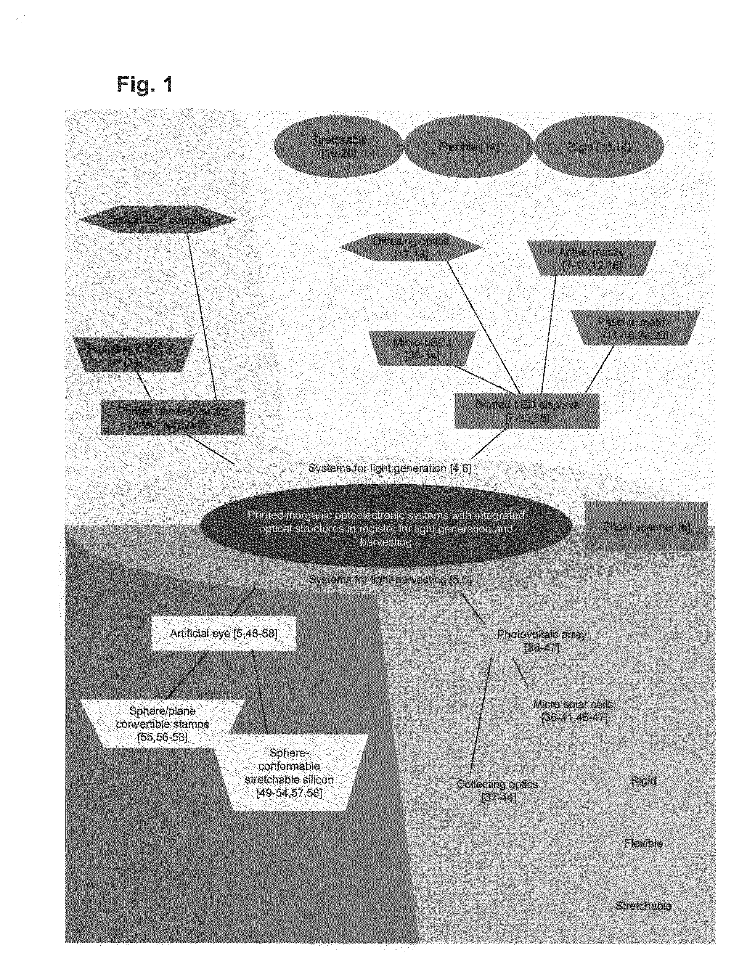
Ultra Thin Flexible Solar (UTFS) Devices and Methods
[0168]Photovoltaic (PV) energy conversion is the direct conversion of sunlight into electricity using a semiconductor device structure. The most common technology in the PV industry is based on single crystalline and polycrystalline silicon technology. Presently, silicon PV technology has high materials costs, due to the relatively inefficient use of the bulk silicon material. In conventional methods, bulk crystalline silicon is sawn into wafers, which are then processed into solar cells and soldered together to form the final module. Typical multicrystalline efficiencies are on the order of 15%; high-performance, single-crystal silicon has been produced with 20% efficiency. For this type of solar cell, 57% of the cost is in materials, and of that total material cost 42% comes from the crystalline Si. In addition, these modules are rigid and heavy.
[0169]There is currently interest in thin-film PV technologies, since these systems h...
example 2
Conformable Thin Film LED Lighting Systems
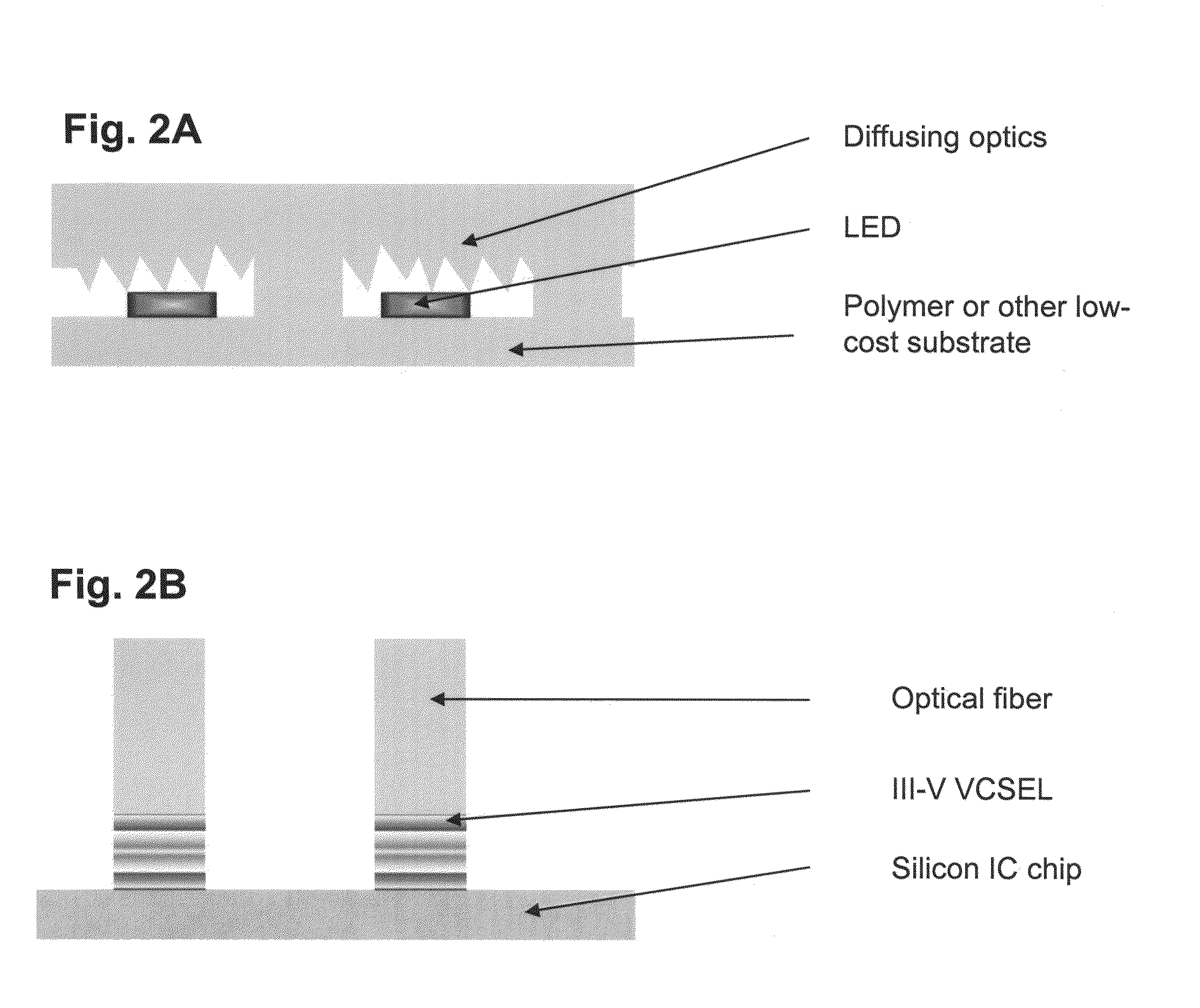
[0194]The present invention provides printing based techniques that provide a means to integrate inorganic light emitting diodes with thin flexible substrates. This approach, as implemented with automated high precision printer systems, is useful for fabricating light-weight and mechanically conformable interior lighting elements for automotive and other applications, in a manner that is compatible with low cost manufacturing.
[0195]The present methods and systems involve fabrication of conformable ILED-based thin film lighting devices followed by application to surfaces using adhesive bonding. Methods may also optionally include processing involving incorporation of encapsulation and planarizing materials, coatings and layers to enhance mechanical properties of the system. The sizes of the thin film structures, the numbers and spacings of the ILEDs and other aspects determine the device designs for specific application.
[0196]Transfer printin...
example 3
Printing-Based Assembly of Solar Cells and Solar Cell Arrays
[0207]FIG. 44 provides a schematic for the formation of a micro single crystal silicon solar cell with low-level concentrating lens. In the first step (a) the micro structures are transferred from PDMS onto an embedded electrode which serves as the back electrical contact for the device. The silicon is transferred by laminating the PDMS onto the electrode surface and slowly peeling the PDMS back. Next, in step (b), planarization followed by the formation of the top metal contacts is performed. The device is completed by integrating a low concentration cylindrical lens array made from PDMS onto the device (step c). In this final step it can be seen that the device was designed such that the rows of silicon cells align with the focal point of the lens array.
[0208]FIG. 45 provides images of a silicon solar cell transferred to a glass substrate. (a) Optical image of a single cell on a glass substrate with both top and bottom el...
PUM
 Abstract
Description
Claims
Application Information