Method of manufacturing a semiconductor device having a reverse staggered thin film transistor

a technology of reverse staggered thin film and semiconductor devices, which is applied in the direction of semiconductor devices, basic electric elements, electrical appliances, etc., can solve the problems of non-uniform luminance of light-emitting display devices using tft using amorphous semiconductor films as switching for pixels, limited application prospects, and difficult realization of liquid crystal display devices in ocb mode. achieve the effect of low cost, low resistance and high reliability

Inactive Publication Date: 2011-08-23
SEMICON ENERGY LAB CO LTD
View PDF36 Cites 22 Cited by
  • Summary
  • Abstract
  • Description
  • Claims
  • Application Information

AI Technical Summary

Benefits of technology

[0165]Although heat-resistance and effect of hillock suppression can not be adequately obtained by a conventional single layer structure of a film containing aluminum as its main component (including a film containing carbon and the like), the problem can be solved according to the present invention by forming another conductive film over the film containing aluminum as its main component. That is, a reverse staggered TFT having a crystalline semiconductor film can be formed using a gate electrode with low resistance, high reliability, and low cost, and can be provided for a large area device.
[0166]According to the invention, a TFT can be formed with a few masks. Since the TFT of the invention is formed of a crystalline semiconductor film, the TFT has high mobility compared to a reverse staggered TFT formed of an amorphous semiconductor film. Further, a source region and a drain region include a catalytic element in addition to an acceptor-type element and a donor-type element. Therefore, a source region and a drain region with low resistivity can be formed. As a result, a semiconductor device which requires high-speed operation can be manufactured. A liquid crystal display device capable of high response speed and display with a large viewing angle, such as an OCB mode can be manufactured.
[0167]Furthermore, variation in characteristics of the TFT can be reduced since deviation of threshold is hard to occur compared with a TFT formed of an amorphous semiconductor film. Accordingly, image irregularity can be reduced compared with an EL display device using the TFT formed of the amorphous semiconductor film as a switching element; thereby a semiconductor device with higher reliability can be manufactured.
[0168]Moreover, since a metal element mixed into a semiconductor film in a film formation stage is also gettered by a gettering process, off current can be reduced. Therefore, contrast can be improved by using such a TFT as a switching element of a display device, for example, a liquid crystal display device.
[0169]Liquid crystal television and EL television having a semiconductor device formed by the above mentioned manufacturing steps can be manufactured with higher throughput and yield, and lower cost.
[0170]Hereinafter, the best modes for carrying out the invention are described with reference to drawings. However, the present invention can be carried out in many different modes, and it is easily understood by those of ordinary skill in the art that the modes and the detail can be changed variously unless otherwise such changes and modifications depart from the scope of the present invention. Note that, portions identical to each other are denoted by same reference numerals in each drawing, and will not be further explained.

Problems solved by technology

However, a TFT using an amorphous semiconductor film has its limits.
For example, a liquid crystal display device in an OCB mode becomes difficult to be realized.
Therefore, a light-emitting display device which uses a TFT using an amorphous semiconductor film as switching for pixels has non-uniform luminance.
There arises a serious problem of deterioration of image quality.
However, aluminum has the problem of heat resistance.
Generation of the hillock (void) causes short-circuit between wirings or breaking of wirings and deterioration of reliability.

Method used


Image

  • Method of manufacturing a semiconductor device having a reverse staggered thin film transistor
  • Method of manufacturing a semiconductor device having a reverse staggered thin film transistor
  • Method of manufacturing a semiconductor device having a reverse staggered thin film transistor

Examples


embodiment mode 1

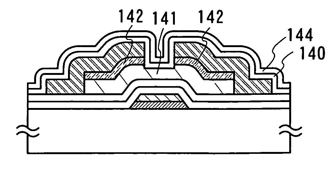
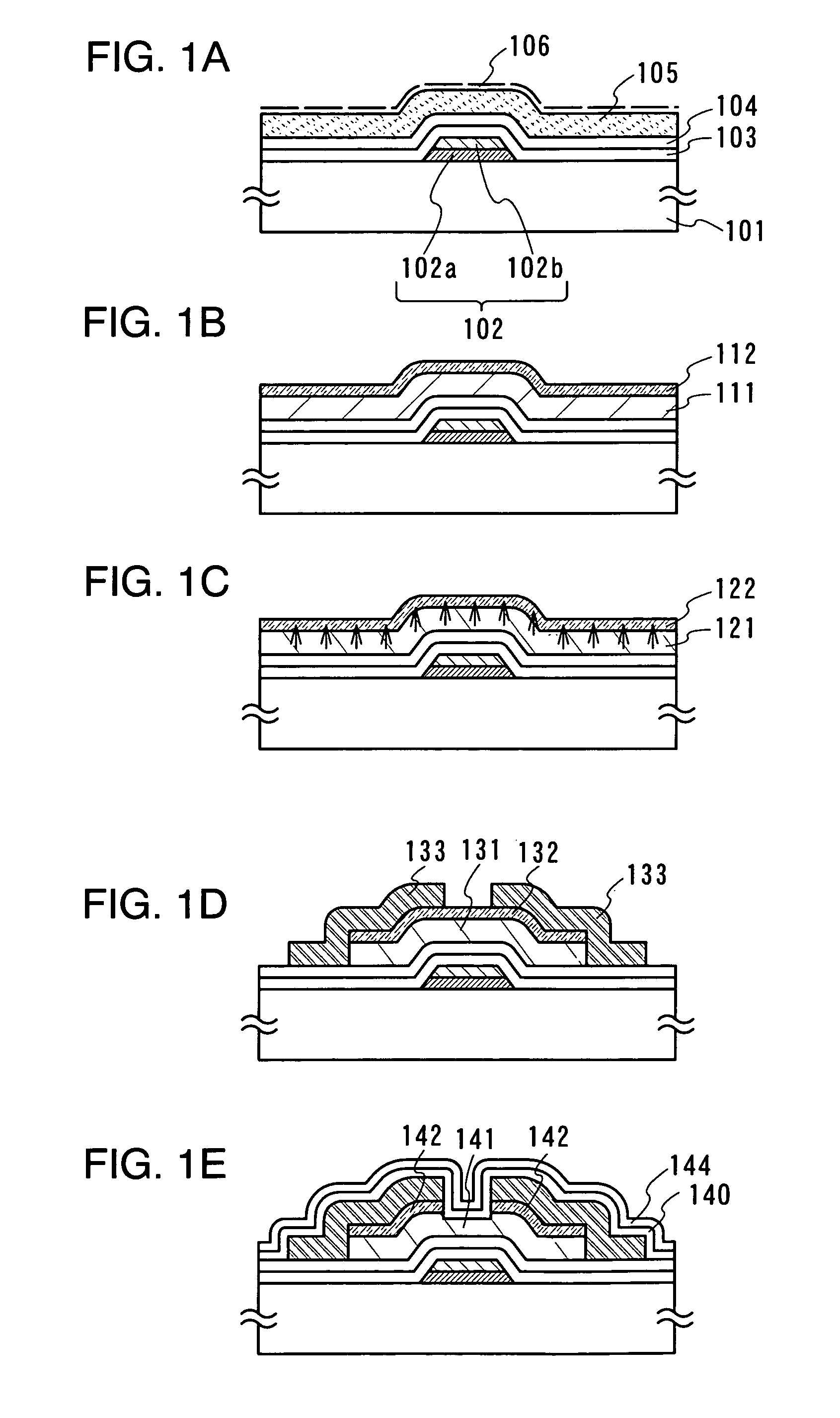
[0197]In this embodiment mode, manufacturing steps of a reverse staggered TFT having a crystalline semiconductor film is described with reference to FIGS. 1A to 1E.

[0198]As shown in FIG. 1A, a first conductive film 102a is formed over a substrate 101, and a second conductive film 102b is formed thereover. Then, a first insulating film 103 and a second insulating film 104 are formed over the second conductive film 102b. A first semiconductor film 105 is formed over the second insulating film 104, and a layer 106 including a catalytic element is formed over the first semiconductor film 105.

[0199]Note that a base film may be formed between the substrate 101 and the first conducive film 102a if necessary so as to prevent impurities from a substrate side and the like from being diffused. As the base film, silicon oxide (SiOx), silicon nitride (SiNx), silicon oxynitride (SiOxNy(x>y)), silicon nitride oxide (SiNxOy(x>y)), or the like can be used appropriately.

[0200]As the substrate 101, a ...

embodiment mode 2

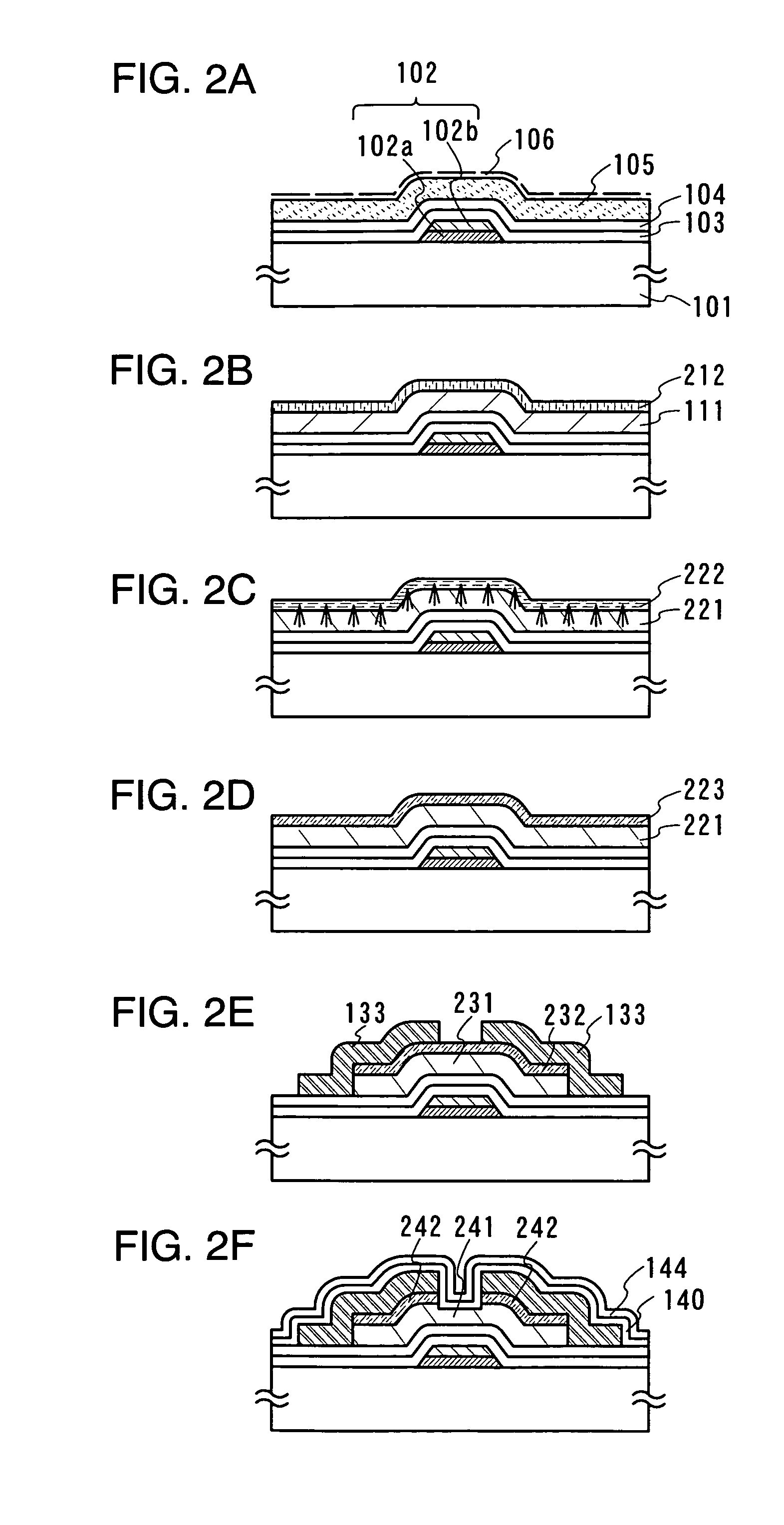
[0231]In this embodiment mode, a step of forming a TFT by conducting gettering to a catalytic element using a semiconductor film including an inert gas element as a substitute for a semiconductor film having a donor-type element is described with reference to FIGS. 2A to 2F.

[0232]As shown in FIGS. 2A and 2B, a first crystalline semiconductor film 111 is formed using the similar step to Embodiment Mode 1. Hereafter, a channel doping step may be conducted. Then, an oxide film with a film thickness of 1 to 5 nm may be formed on the surface of the first crystalline semiconductor film. Here, an oxide film is formed by applying ozone water over the surface of the crystalline semiconductor film.

[0233]Then, a second semiconductor film 212 having a rare gas element is formed over the first crystalline semiconductor film 111 by a known method such as a PVD method or a CVD method. As the second semiconductor film 212, an amorphous semiconductor film is preferably used.

[0234]Subsequently, the f...

embodiment mode 3

[0239]In this embodiment mode, a step of forming an n-channel TFT and a p-channel TFT over the same substrate is described with reference to FIGS. 3A to 3D.

[0240]As shown in FIG. 3A, as with Embodiment Mode 1, a gate electrode 301 (which is formed of a first conductive film 301a and a second conductive film 301b) and a gate electrode 302 (which is formed of a first conductive film 302a and a second conductive film 302b) are formed over a substrate 101, and a first insulating film 103 and a second insulating film 104 are formed over the gate electrode 301 and the gate electrode 302. Using the same steps as Embodiment Mode 1, a first crystalline semiconductor film is formed and a second semiconductor film including a donor-type element is formed thereover. Using a mask formed by a photolithography process, the first crystalline semiconductor film is etched into a desired shape to form a first semiconductor region, and a second semiconductor film is etched into a desired shape to form ...


PUM

PropertyMeasurementUnit
angleaaaaaaaaaa
angleaaaaaaaaaa
angleaaaaaaaaaa

Abstract

A gate electrode is formed by forming a first conductive layer containing aluminum as its main component over a substrate, forming a second conductive layer made from a material different from that used for forming the first conductive layer over the first conductive layer; and patterning the first conductive layer and the second conductive layer. Further, the first conductive layer includes one or more selected from carbon, chromium, tantalum, tungsten, molybdenum, titanium, silicon, and nickel. And the second conductive layer includes one or more selected from chromium, tantalum, tungsten, molybdenum, titanium, silicon, and nickel, or nitride of these materials.

Description

BACKGROUND OF THE INVENTION[0001]1. Technical Field[0002]The present invention relates to a method for manufacturing a semiconductor device having a reverse staggered thin film transistor including a crystalline semiconductor film.[0003]2. Background Art[0004]In recent years, a flat panel display (FPD) as typified by a liquid crystal display (LCD) or an EL (Electro Luminescence) display has attracted attention as a display device which can take the place of the conventional CRT. Particularly, the development of a large screen liquid crystal television mounted with an active matrix large liquid crystal panel is an important issue which should be focused by a liquid crystal panel manufacturer. A large screen EL television has been developed in recent years following the development of a liquid crystal television.[0005]In the conventional liquid crystal display device or EL display device (hereinafter, light-emitting display device), a thin film transistor (hereinafter, TFT) using an a...

Claims


Application Information

Patent Timeline
Patent Type & Authority Patents(United States)
IPC IPC(8): H01L21/00H01L21/84
CPCH01L21/3221H01L27/1277H01L29/66765H01L29/78678H01L27/124H01L29/4908H01L21/2022H01L21/2026H01L21/02422H01L21/02532H01L21/02672
Inventor AKIMOTO, KENGOMARUYAMA, HOTAKA
Owner SEMICON ENERGY LAB CO LTD
Why Eureka
Try Eureka