[0010]An objective of the disclosure is to overcome the drawbacks of prior art, i.e., complex structure, strict process requirement, low feasibility and bad heat dissipation of heat dissipation substrate in power LEDs, and low
manufacturing efficiency, bad product consistency and reliability, and high product cost of the power LED devices.
[0011]Another objective of the disclosure is to provide a heat dissipation substrate with a heat sink assembled in a circuit board, and a power LED device including the heat dissipation substrate. The heat dissipation substrate has a simple structure, is easy to manufacture, lowers
process requirements and can effectively solve heat dissipation problems of the power LED devices, especially that of high power LED devices. The device manufactured by the heat dissipation substrate has good consistency, high reliability and good heat dissipation. The device still has high production efficiency, simple structure, low product cost, and can boost the power of power LEDs. It can ensure that the power LED product according to the disclosure will satisfy the booming market.
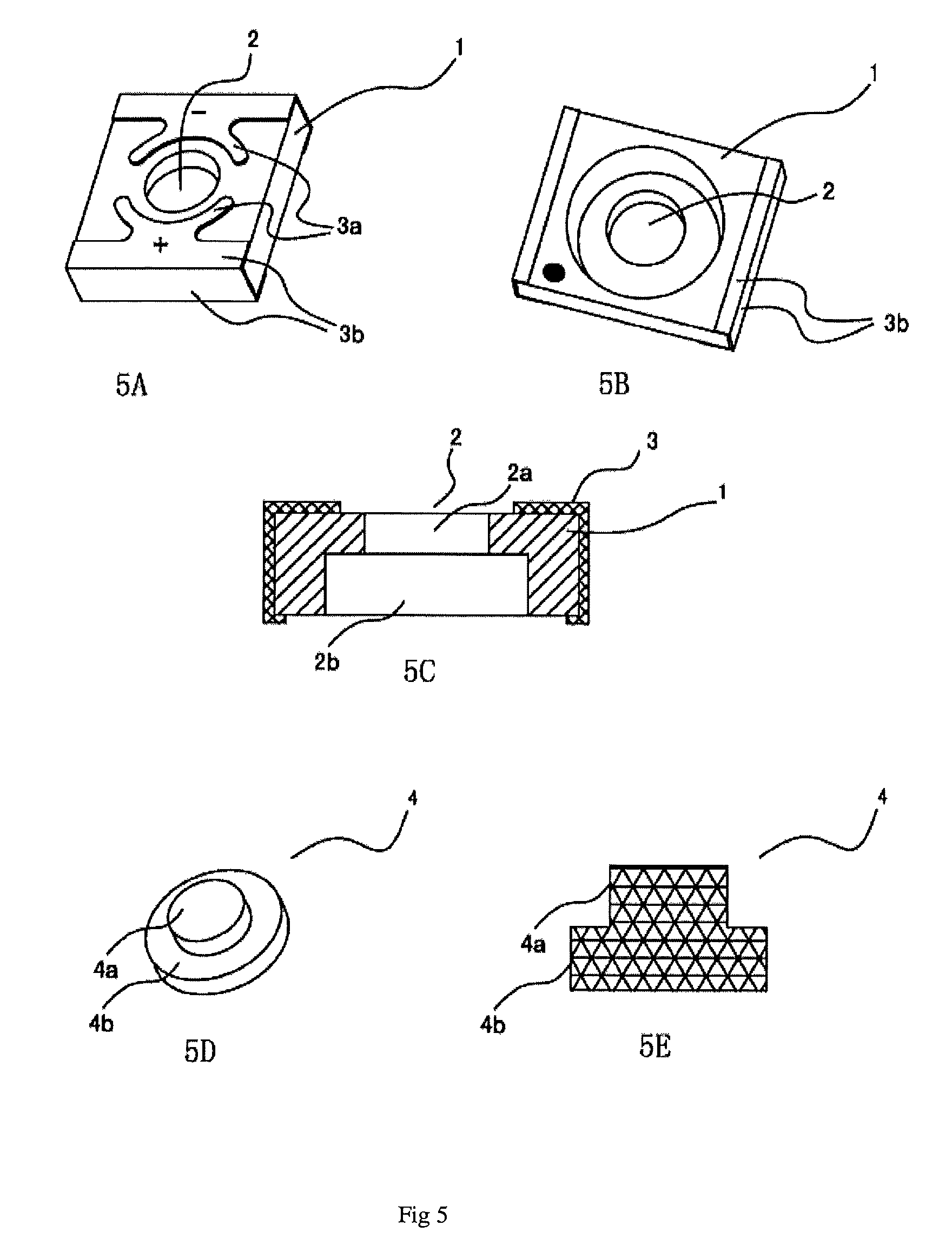
[0012]To achieve the above objectives, a structure of heat dissipation substrate used for manufacturing a power LED is provided. The structure of heat dissipation substrate comprises: a circuit board, said circuit board being of an one-piece structure and with a counterbore and
metal lines arranged thereon, wherein the counterbore is structured as a through hole and a
blind hole communicating with each other, the through hole is smaller than the blind hole, and the axis direction of both the through hole and the blind hole are the same; The heat sink has an one-piece terraced structure formed by an upper terrace and a lower terrace, wherein the
diameter of the upper terrace is close to the aperture of the through hole and the
diameter of the lower terrace is close to the aperture of the blind hole, the height of the lower terrace of the heat sink is greater than or equal to the depth of the blind hole, the upper terrace and the lower terrace share the same direction of axis; the heat sink matches in structure with the counterbore, and the heat sink can be embedded firmly in the counterbore. Due to its one-piece structure, the structure of heat dissipation substrate simplifies complex multilayer structure existing in prior art circuit board and effectively ensures
process quality of the heat dissipation substrate. The heat sink and the circuit board are structured to enable a remarkably simple process for assembling the heat sink in the counterbore of the heat dissipation substrate, by which the heat sink can be firmly fit, reliably positioned and uneasy to slip, thus the
assembly quality is highly guaranteed. Furthermore, the lower terrace in the one-piece structure of the head sink has a volume bigger than that of the upper terrace, providing a heat sink with bigger thermal capacity and larger heat dissipation area; when assembled in the counterbore, the bottom of the heat sink is flush with or it extrudes from the
printed circuit board so that the heat sink may be enabled to contact with other heat-transfer medium to dissipate the heat, thus achieving a very good heat dissipation and greatly boosting the development of power LED. The power LED is designed to deliver high power. The heat dissipation substrate has a simple structure, is easy to manufacture and greatly reduces product cost of the heat dissipation substrate of the power LED.
[0013]To achieve the above objectives, the device also provides a second heat dissipation substrate having a plurality of counterbores and heat sinks, with the heat dissipation substrate mentioned above acting as a basic element thereof. The second heat dissipation substrate has a one-piece circuit board, at terminating ends of which position lines for
cutting are placed and within which slots and / or holes are placed. In the circuit board, an array, M column×N rows, of counterbores is placed, wherein M and N are respectively integers more than or equal to 1, and M and N cannot be equal to 1 simultaneously. Each of the heat sinks is in an
interference fit with the corresponding counterbore of the array of counterbores. This second structure of heat dissipation substrate overcomes drawbacks existing in manufacturing process of power LEDs, such as, complex processes, power LEDs being manufactured piece by piece and bad consistency of product. By simple design of the heat dissipation substrate, a plurality of power LEDs can be manufactured on the same heat dissipation substrate. When manufacturing LED devices from the heat dissipation substrate, the substrate is first encapsulated with
colloid and then
cut along the position lines for
cutting so that the encapsulated LED products can be divided into independent LED devices. The device simplifies manufacturing process of power LED devices, with production efficiency enhanced, production cost reduced, and good consistency of product quality achieved.
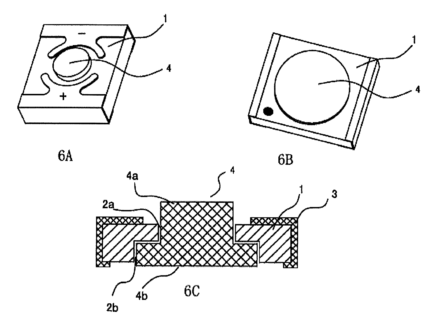
[0014]In order to meet the above objectives, the device provides a power LED device manufactured by using the above heat dissipation substrate of power LED. The power LED device comprises a heat sink, the circuit board with a counterbore, a LED
chip, bonding wires, and an encapsulation
colloid, wherein the heat sink is in an
interference fit with the counterbore of the circuit board, the LED
chip is mounted on the heat sink, the lines of the circuit board, having internal wire connection parts and external electrodes, act as device electrodes, with the bonding wires connecting LED
chip electrodes to the internal wire connection parts on the circuit board. Then, the encapsulation
colloid is used to cover the side of the circuit board carrying the chip, keeping the external electrodes outside. The encapsulation colloid functions not only as a sealing layer for sealing the chip and the bonding wires from outside
moisture and air, but also as an optical lens integrated with the device. The above power LED device manufactured by using the heat dissipation substrate has desirable heat dissipation, enabling a great power boost of the power LED device. It can be manufactured in batches due to the heat dissipation substrate structure and simple encapsulation, providing good consistence for the power LED devices and achieving high production efficiency. More importantly, due to the fact that the encapsulation colloid functions as an one-shot forming optical lens, the light extracting characteristic of the power LED device has been improved when compared to a prior art device with lens assembled on encapsulation colloid. The power LED device has a simple and compact structure, high product reliability, and low production cost. Because the heat dissipation substrate has a good characteristic of heat dissipation, the power LED device manufactured by using the heat dissipation substrate of the invention can use more power. Thus the device can yield a LED device using high power. Using the simple and practical design of the heat dissipation substrate adopting the counterbore and heat sink, complex
manufacturing technology of LED can be simplified, production efficiency of a power LED device can be greatly improved and the lifetime of a power LED device can be extended.

